AD7858/AD7858L
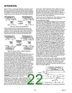
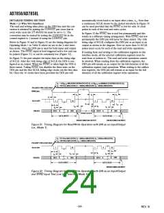
The timing diagram for a system offset or system gain calibra-
tion is shown in Figure 30. Here again the CAL is pulsed and
the rising edge of the CAL initiates the calibration sequence (or
the calibration can be initiated in software by writing to the
control register). The rising edge of the CAL causes the BUSY
line to go high and it will stay high until the calibration se-
quence is finished. The analog input should be set at the correct
level for a minimum setup time (tSETUP) of 100 ns before the rising
edge of CAL and stay at the correct level until the BUSY signal
goes low.
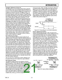
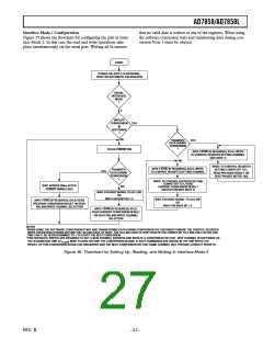
Resetting the Serial Interface
When writing to the part via the DIN line there is the possibility
of writing data into the incorrect registers, such as the test regis-
ter for instance, or writing the incorrect data and corrupting the
serial interface. The SYNC pin acts as a reset. Bringing the
SYNC pin high resets the internal shift register. The first data
bit after the next SYNC falling edge will now be the first bit of a
new 16-bit transfer. It is also possible that the test register con-
tents were altered when the interface was lost. Therefore, once
the serial interface is reset it may be necessary to write the 16-bit
word 0100 0000 0000 0010 to restore the test register to its
default value. Now the part and serial interface are completely
reset. It is always useful to retain the ability to program the
SYNC line from a port of the µController/DSP to have the
ability to reset the serial interface.
t1
CAL (I/P)
t15
BUSY (O/P)
Table X summarizes the interface modes provided by the
AD7858/AD7858L. It also outlines the various µP/µC to which
the particular interface is suited.
tCAL2
tSETUP
V
OR V
SYSTEM OFFSET
AIN (I/P)
SYSTEM FULL SCALE
Interface Mode 1 may only be set by programming the control
register (see section on Control Register).
Figure 30. Timing Diagram for System Gain or System
Offset Calibration
Some of the more popular µProcessors, µControllers, and the
DSP machines that the AD7858/AD7858L will interface to
directly are mentioned here. This does not cover all µCs, µPs,
and DSPs. A more detailed timing description on each of the
interface modes follows.
SERIAL INTERFACE SUMMARY
Table IX details the two interface modes and the serial clock
edges from which the data is clocked out by the AD7858/
AD7858L (DOUT Edge) and that the data is latched in on
(DIN Edge).
Table X. Interface Mode Description
In both interface Modes 1 and 2 the SYNC is gated with the
SCLK. Thus the SYNC↓ may clock out the MSB of data. Sub-
sequent bits will be clocked out by the Serial Clock, SCLK. The
condition for the SYNC↓ clocking out the MSB of data is as
follows:
Interface
Mode
Processor/
Controller
Comment
1
8XC51
8XL51
PIC17C42
(2-Wire)
(DIN Is an Input/
Output Pin)
The falling edge of SYNC will clock out the MSB if the serial clock
is low when the SYNC goes low.
2
68HC11
68L11
68HC16
PIC16C64
ADSP21xx
DSP56000
DSP56001
DSP56002
DSP56L002
(3-Wire, SPI)
(Default Mode)
If this condition is not the case, the SCLK will clock out the
MSB. If a noncontinuous SCLK is used, it should idle high.
Table IX. SCLK Active Edges
Interface Mode
Edge
DOUT Edge
DIN
1, 2
SCLK↓
SCLK↑
REV. B
–23–

 ADI [ ADI ]