AD7858/AD7858L
AD7858/AD7858L to DSP56000/1/2/L002 Interface
A typical sequence of events would be to write to the control
register via the DIN line setting a conversion start and at the
same time reading data from the previous conversion on the
DOUT line (both the read and write operations would each be
two 8-bit operations, one 16-bit operation for the 68HC16),
wait for the conversion to be finished (= 4.6 µs for AD7858
with 4 MHz CLKIN), and then repeat the sequence. The maxi-
mum serial frequency will be determined by the data access and
hold times of the µControllers and the AD7858/AD7858L.
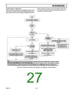
Figure 40 shows the AD7858/AD7858L to DSP56000/1/2/
L002 interface. Here the DSP5600x is the master and the
AD7858 is the slave. The AD7858/AD7858L is in Interface
Mode 2. The DSP56L002 is used when the AD7858/AD7858L
is being operated at 3 V. The setting of the bits in the registers
of the DSP5600x would be for synchronous operation (SYN =
1), internal frame sync (SCD2 = 1), gated internal clock (GCK
= 1, SCKD = 1), 16-bit word length (WL1 = 1, WL0 = 0). Since
a gated clock is used here the SCLK cannot be tied to the CLKIN
of the AD7858/AD7858L. The SCLK from the DSP5600x
must be inverted before it is applied to the AD7858/AD7858L.
Again the data access and hold times of the DSP5600x and
the AD7858/AD7858L allows for a SCLK of 4 MHz/1.8 MHz.
AD7858/AD7858L to ADSP-21xx Interface
Figure 39 shows the AD7858/AD7858L interface to the ADSP-
21xx. The ADSP-21xx is the master and the AD7858/AD7858L
is the slave. The AD7858/AD7858L is in Interface Mode 2.
For the ADSP-21xx the bits in the serial port control register
should be set up as TFSR = RFSR = 1 (need a frame sync for
every transfer), SLEN = 15 (16-bit word length), TFSW =
RFSW = 1 (alternate framing mode for transmit and receive
operations), INVRFS = INVTFS = 1 (active low RFS and
TFS), IRFS = 0, ITFS = 1 (External RFS and internal TFS),
and ISCLK = 1 (internal serial clock). The CLKIN and
CONVST signals can be supplied from the ADSP-21xx or
from an external source. The serial clock from the ADSP-21xx
must be inverted before the SCLK pin of the AD7858/AD7858L.
This SCLK could also be used to drive the CLKIN input of the
AD7858/AD7858L. The BUSY signal indicates when the con-
version is finished and may not be required. The data access
and hold times of the ADSP-21xx and the AD7858/AD7858L
allow for a serial clock of 4 MHz/1.8 MHz at 5 V and 3.3 MHz/
1.8 MHz at 3 V supplies.
OPTIONAL
AD7858/AD7858L
CONVST
4MHz/1.8MHz
DSP56000/1/2/L002
CLKIN
SCK
SRD
SC2
SCLK
DOUT
SYNC
SLAVE
MASTER
OPTIONAL
IRQ
BUSY
DIN
STD
Figure 40. DSP56000/1/2 Interface
OPTIONAL
AD7858/AD7858L
CONVST
4MHz/1.8MHz
CLKIN
SCLK
DOUT
SYNC
ADSP-21xx
SCK
DR
RFS
TFS
IRQ
MASTER
SLAVE
OPTIONAL
BUSY
DIN
DT
Figure 39. ADSP-21xx Interface
REV. B
–29–

 ADI [ ADI ]