AD7858/AD7858L
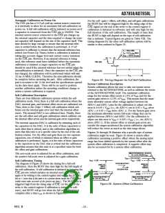
Automatic Calibration on Power-On
For the self- (gain + offset), self-offset, and self-gain calibrations
the BUSY line will be triggered high by the rising edge of the
CAL signal (or the end of the write to the control register if
calibration is initiated in software) and will stay high for the
full duration of the self-calibration. The length of time that
the BUSY is high will depend on the type of self-calibration
that is initiated. Typical figures are given in Table VIII. The
timing diagrams for the other self-calibration options will be
similar to that outlined in Figure 25.
The CAL pin has a 0.15 µA pull-up current source connected
to it internally to allow for an automatic full self-calibration on
power-on. A full self-calibration will be initiated on power-on if
a capacitor is connected from the CAL pin to DGND. The
internal current source connected to the CAL pin charges up
the external capacitor and the time required to charge the exter-
nal capacitor will depend on the size of the capacitor itself. This
time should be large enough to ensure that the internal refer-
ence is settled before the calibration is performed. A 33 nF
capacitor is sufficient to ensure that the internal reference has
settled (see Power-Up Times) before a calibration is initiated
taking into account trigger level and current source variations
on the CAL pin. However, if an external reference is being
used, this reference must have stabilized before the automatic
calibration is initiated (a larger capacitor on the CAL pin
should be used if the external reference has not settled when the
autocalibration is initiated). Once the capacitor on the CAL pin
has charged, the calibration will be performed which will take
32 ms (4 MHz CLKIN). Therefore the autocalibration should
be complete before operating the part. After calibration, the
part is accurate to the 12-bit level and the specifications quoted
on the data sheet apply. There will be no need to perform
another calibration unless the operating conditions change or
unless a system calibration is required.
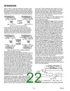
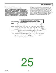
t1 = 100ns MIN,
t15 = 2.5 tCLKIN MAX,
tCAL = 125013 tCLKIN
t1
CAL (I/P)
t15
BUSY (O/P)
tCAL
Figure 25. Timing Diagram for Full Self-Calibration
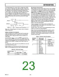
System Calibration Description
System calibration allows the user to take out system errors
external to the AD7858/AD7858L as well as calibrate the errors
of the AD7858/AD7858L itself. The maximum calibration
range for the system offset errors is 5% of VREF and for the
system gain errors is 2.5% of VREF. This means that the maxi-
mum allowable system offset voltage applied between the
AIN(+) and AIN(–) pins for the calibration to adjust out this
error is 0.05 × VREF (i.e., the AIN(+) can be 0.05 × VREF above
AIN(–) or 0.05 × VREF below AIN(–)). For the System gain error
the maximum allowable system full-scale voltage that can be
applied between AIN(+) and AIN(–) for the calibration to
adjust out this error is VREF 0.025 × VREF ( i.e., the AIN(+)
above AIN(–)). If the system offset or system gain errors are
outside the ranges mentioned the system calibration algorithm
will reduce the errors as much as the trim range allows.
Self-Calibration Description
There are four different calibration options within the self-
calibration mode. First, there is a full self-calibration where the
DAC, internal gain, and internal offset errors are calibrated out.
Then, there is the (Gain + Offset) self-calibration which cali-
brates out the internal gain error and then the internal offset
errors. The internal DAC is not calibrated here. Finally, there
are the self-offset and self-gain calibrations which calibrate out
the internal offset errors and the internal gain errors respectively.
The internal capacitor DAC is calibrated by trimming each of
the capacitors in the DAC. It is the ratio of these capacitors to
each other that is critical, and so the calibration algorithm en-
sures that this ratio is at a specific value by the end of the cali-
bration routine. For the offset and gain there are two separate
capacitors, one of which is trimmed when an offset or gain
calibration is performed. Again, it is the ratio of these capacitors
to the capacitors in the DAC that is critical and the calibration
algorithm ensures that this ratio is at a specified value for both
the offset and gain calibrations.
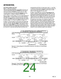
Figures 26 through 28 illustrate why a specific type of system
calibration might be used. Figure 26 shows a system offset
calibration (assuming a positive offset) where the analog input
range has been shifted upwards by the system offset after the
system offset calibration is completed. A negative offset may
also be accounted for by a system offset calibration.
MAX SYSTEM FULL SCALE
The zero-scale error is adjusted for an offset calibration, and
the positive full-scale error is adjusted for a gain calibration.
IS ؎2.5% FROM V
REF
V
+ SYS OFFSET
REF
V
–1LSB
V
– 1LSB
REF
Self-Calibration Timing
REF
SYSTEM OFFSET
CALIBRATION
The diagram of Figure 25 shows the timing for a full self-
calibration. Here the BUSY line stays high for the full length of
the self-calibration. A self-calibration is initiated by bringing the
CAL pin low (which initiates an internal reset) and then high
again or by writing to the control register and setting the STCAL
bit to 1 (note that if the part is in a power-down mode the CAL pulse-
width must take account of the power-up time ). The BUSY line is
triggered high from the rising edge of CAL (or the end of the
write to the control register if calibration is initiated in soft-
ware), and BUSY will go low when the full self-calibration is
complete after a time tCAL as shown in Figure 25.
ANALOG
INPUT
ANALOG
INPUT
RANGE
RANGE
SYS OFFSET
AGND
SYS OFFSET
AGND
MAX SYSTEM OFFSET
IS ؎5% OF V
MAX SYSTEM OFFSET
IS ؎5% OF V
REF
REF
Figure 26. System Offset Calibration
REV. B
–21–

 ADI [ ADI ]