AD7858/AD7858L
DETAILED TIMING SECTION
Mode 1 (2-Wire 8051 Interface)
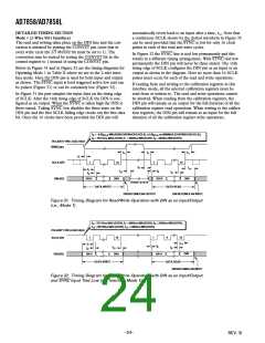
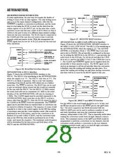
automatically revert back to an input after a time, t14. Note that
a continuous SCLK shown by the dotted waveform in Figure 35
can be used provided that the SYNC is low for only 16 clock
pulses in each of the read and write cycles.
The read and writing takes place on the DIN line and the con-
version is initiated by pulsing the CONVST pin (note that in
every write cycle the 2/3 MODE bit must be set to 1). The
conversion may be started by setting the CONVST bit in the
control register to 1 instead of using the CONVST pin.
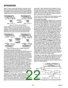
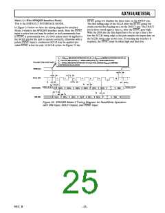
In Figure 32 the SYNC line is tied low permanently and this
results in a different timing arrangement. With SYNC tied low
permanently the DIN pin will never be three-stated. The 16th
rising edge of SCLK configures the DIN pin as an input or an
output as shown in the diagram. Here no more than 16 SCLK
pulses must occur for each of the read and write operations.
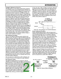
Below in Figure 31 and in Figure 32 are the timing diagrams for
Operating Mode 1 in Table X where we are in the 2-wire inter-
face mode. Here the DIN pin is used for both input and output
as shown. The SYNC input is level triggered active low and can
be pulsed (Figure 31) or can be constantly low (Figure 32).
If reading from and writing to the calibration registers in this
interface mode, all the selected calibration registers must be
read from or written to. The read and write operations cannot
be aborted. When reading from the calibration registers, the
DIN pin will remain as an output for the full duration of all the
calibration register read operations. When writing to the calibra-
tion registers, the DIN pin will remain as an input for the full
duration of all the calibration register write operations.
In Figure 31 the part samples the input data on the rising edge
of SCLK. After the 16th rising edge of SCLK the DIN is con-
figured as an output. When the SYNC is taken high the DIN is
three-stated. Taking SYNC low disables the three-state on the
DIN pin and the first SCLK falling edge clocks out the first data
bit. Once the 16 clocks have been provided the DIN pin will
t3 = –0.4tSCLK MIN (NONCONTINUOUS SCLK) ؎0.4tSCLK ns MIN/MAX (CONTINUOUS SCLK),
t6 = 75/115ns MAX (5V/3V), t7 = 40/60ns MIN (5V/3V), t8 = 20/30ns MIN (5V/3V)
POLARITY PIN LOGIC HIGH
SYNC (I/P)
t11
t3
t11
t3
1
16
1
16
SCLK (I/P)
t5
t14
t7
t8
t6
t12
t6
DB15
DB0
DB15
DB0
DIN (I/O)
THREE-STATE
DATA WRITE
DATA READ
DIN BECOMES AN INPUT
DIN BECOMES AN OUTPUT
Figure 31. Timing Diagram for Read/Write Operation with DIN as an Input/Output
(i.e., Mode 1)
t6 = 75/115ns MAX (5V/3V), t7 = 40/60ns MIN (5V/3V), t8 = 20/30ns MIN (5V/3V),
t13 = 90/130ns MAX (5V/3V), t14 = 50/90ns MIN (5V/3V)
POLARITY PIN LOGIC HIGH
1
16
1
6
16
SCLK (I/P)
t14
t7
t8
t6
t13
DB0
t6
DB0
DIN (I/O)
DB15
DB15
DATA WRITE
DATA READ
DIN BECOMES AN INPUT
Figure 32. Timing Diagram for Read/Write Operation with DIN as an Input/Output
and SYNC Input Tied Low (i.e., Interface Mode 1)
–24–
REV. B

 ADI [ ADI ]