AD7575
A SAMPLED-DATA INPUT
40
42
44
46
48
50
52
54
T
= +25؇C
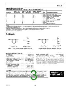
The AD7575 makes use of a sampled-data comparator. The
equivalent input circuit is shown in Figure 9. When a conversion
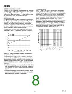
starts, switch S1 is closed, and the equivalent input capacitance
is charged to VIN. With a switch resistance of typically
500 Ω and an input capacitance of typically 2 pF, the input time
constant is 1 ns. Thus CIN becomes charged to within ±1/4 LSB
in 6.9 time constants or about 7 ns. Since the AD7575 requires
two input clock cycles (at a clock frequency of 4 MHz) before
going into the compare mode, there is ample time for the input
voltage to settle before the first comparator decision is made.
Increasing the source resistance increases the settling time re-
quired. Input bypass capacitors placed directly at the analog
input act to average the input charging currents. The average
current flowing through any source impedance can cause
full-scale errors.
A
100
1k
10k
100k
INPUT FREQUENCY – Hz
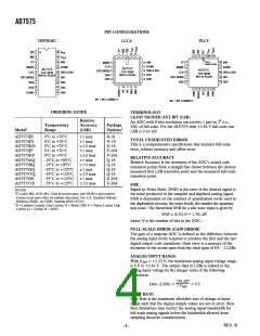
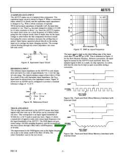
Figure 11. SNR vs. Input Frequency
R
ON
S1
500⍀
V
IN
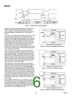
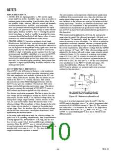
The input signal is held on the third falling edge of the input
clock after CS and RD go LOW. This is indicated in Figure 12
for the Slow Memory Interface. Between conversions, the input
signal is tracked by the AD7575 track-and-hold. Since the
sampled signal is held on a small, on-chip capacitor, it is advis-
able that the data bus be kept as quiet as possible during a
conversion.
C
S
2pF
0.5pF
Figure 9. Equivalent Input Circuit
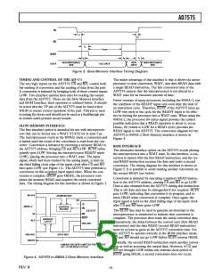
REFERENCE INPUT
The reference input impedance on the AD7575 is code depen-
dent and varies by a ratio of approximately 3-to-1 over the digi-
tal code range. The typical resistance range is from 6 kΩ to 18 kΩ.
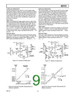
As a result of the code dependent input impedance, the VREF
input must be driven from a low impedance source. Figure 10
shows how an AD589 can be configured to produce a nominal
reference voltage of +1.23 V.
CS
RD
BUSY
+5V
EXTERNAL
CLOCK
3.3k⍀
1.23V
INPUT SIGNAL
HELD HERE
+
47F
0.1F
AD589
–
Figure 12a. Track-and-Hold (Slow Memory Interface) with
External Clock
Figure 10. Reference Circuit
CS
RD
TRACK-AND-HOLD
The on-chip track-and-hold on the AD7575 means that input
signals with slew rates up to 386 mV/µs can be converted with-
out error. This corresponds to an input signal bandwidth of
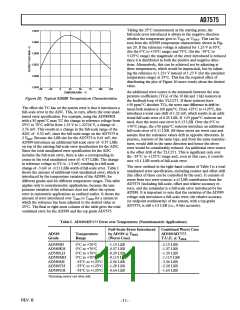
50 kHz for a 2.46 V peak-to-peak sine wave. Figure 11 shows
a typical plot of signal-to-noise ratio versus input frequency over
the input bandwidth of the AD7575. The SNR figures are gen-
erated using a 200 kHz sampling frequency, and the reconstructed
sine wave passes through a filter with a cutoff frequency
of 50 kHz.
BUSY
INTERNAL
CLOCK
INPUT SIGNAL
HELD HERE
The improvement in the SNR figures seen at the higher frequen-
cies is due to the sharp cutoff of the filter (50 kHz, 8th
order Chebyshev) used in the test circuit.
Figure 12b. Track-and-Hold (Slow Memory Interface) with
Internal Clock
REV. B
–7–

 ADI [ ADI ]