AD7575
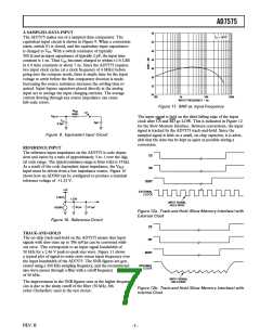
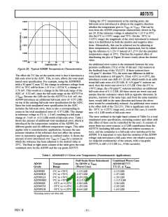
Taking the 25°C measurement as the starting point, the
1.2370
1.2365
1.2360
1.2355
1.2350
1.2345
full-scale error introduced is always in the negative direction
whether the temperature goes to TMIN or TMAX. This can be
seen from the AD589 temperature characteristic shown in Fig-
ure 20. If the reference voltage is adjusted for 1.23 V at 45°C
(for the 0°C to +70°C range) and 75°C (for the –55°C to
+125°C range) the magnitude of the error introduced is reduced
since it is distributed in both the positive and negative direc-
tions. Alternatively, this can be achieved not by adjusting at
these temperatures, which would be impractical, but by adjust-
ing the reference to 1.231 V instead of 1.23 V (for the extended
temperature range) at 25°C. This has the required effect of
distributing the plot of Figure 20 more evenly about the desired
value.
–50
–25
0
25
50
75
100
125
An additional error source is the mismatch between the tem-
perature coefficients (TCs) of the 10 kΩ and 1 kΩ resistors in
the feedback loop of the TLC271. If these resistors have
±50 ppm/°C absolute TCs, the worst case difference in drift be-
tween both resistors is 100 ppm/°C. From +25°C to +125°C, this
introduces a worst case shift of 1.22 mV, which results in an addi-
tional full-scale error of 0.25 LSB. If ±25 ppm/°C resistors are
used, then the worst case error is 0.13 LSB. Over the 0°C to
+70°C range, the ±50 ppm/°C resistors introduce an additional
full-scale error of 0.11 LSB. All these errors are worst case and
assume that the resistance values drift in opposite directions. In
practice, resistors of the same type, and from the same manufac-
turer, would drift in the same direction and hence the above
error would be considerably reduced. An additional error source
is the offset drift of the TLC271. This is significant only over
the –55°C to +125°C range and, even in this case, it contrib-
utes <0.1 LSB worth of full-scale error.
TEMPERATURE – ؇C
Figure 20. Typical AD589 Temperature Characteristics
The effect the TC has on the system error is that it introduces a
full-scale error in the ADC. This, in turn, affects the total unad-
justed error specification. For example, using the AD589KH
with a 50 ppm/°C max TC the change in reference voltage from
25°C to 70°C will be from 1.23 V to 1.22724 V, a change of –
2.76 mV. This results in a change in the full-scale range of the
ADC of –5.52 mV, since the full-scale range on the AD7575 is
2 VREF. Because the LSB size for the AD7575 is 9.61 mV, the
AD589 introduces an additional full-scale error of –0.57 LSBs
on top of the existing full-scale error specification for the ADC.
Since the total unadjusted error specification for the ADC
includes the full-scale error, there is also a corresponding in-
crease in the total unadjusted error of –0.57 LSBs. The change
in reference voltage at 0°C is –1.5 mV, resulting in a full-scale
change of –3 mV or –0.31 LSBs worth of full-scale error. Table I
shows the amount of additional total unadjusted error, which is
introduced by the temperature variation of the AD589, for
different grades and for different temperature ranges. This table
applies only to nonratiometric applications, because the tem-
perature variation of the reference does not affect the system
error in ratiometric applications as outlined earlier. It shows the
amount of error introduced over TMIN to TMAX for a system in
which the reference has been adjusted to the desired value at
25°C. The final or right-most column of the table gives the total
combined error for the AD589 and the top grade AD7575.
The error outlined in the right-hand column of Table I is a total
unadjusted error specification, excluding resistor and offset drift
(the effect of these can be controlled by the user). It consists of
errors from two error sources: a ±l LSB contribution from the
AD7575 (including full-scale, offset and relative accuracy er-
rors), and the remainder is a full-scale error introduced by the
AD589. It is important to note that the variation of the AD589
voltage only introduces a full-scale error; the relative accuracy
(or endpoint nonlinearity) of the system, with a top grade
AD7575, is still ±1/2 LSB (i.e., 8-bits accurate).
Table I. AD589/AD7575 Error over Temperature (Nonratiometric Applications)
Full-Scale Error Introduced
by AD589 @ TMAX
(Worst Case)
Combined Worst Case
AD589/AD7575
T.U.E. @ TMAX
AD589
Grade
Temperature
Range
AD589JH
AD589KH
AD589LH
AD589MH
AD589SH
AD589TH
AD589UH
0°C to +70°C
0°C to +70°C
0°C to +70°C
0°C to +70°C
–55°C to +125°C
–55°C to +125°C
–55°C to +125°C
–1.15 LSB
–0.57 LSB
–0.29 LSB
–0.115 LSB
–2.56 LSB
–1.28 LSB
–0.64 LSB
–2.15 LSB
–1.57 LSB
–1.29 LSB
–1.115 LSB
–3.56 LSB
–2.28 LSB
–1.64 LSB
*Excluding resistor and offset drift.
REV. B
–11–

 ADI [ ADI ]