AD7575
CS
RD
t1
t5
t2
tCONV
BUSY
t6
t7
t3
HIGH IMPEDANCE
BUS
NEW
DATA
HIGH IMPEDANCE
BUS
DATA
OLD DATA
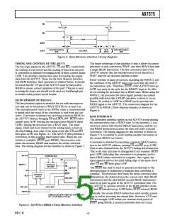
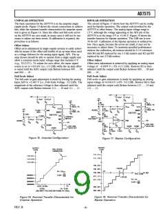
Figure 3. Slow Memory Interface Timing Diagram
The major advantage of this interface is that it allows the micro-
processor to start conversion, WAIT, and then READ data with
a single READ instruction. The fast conversion time of the
AD7575 ensures that the microprocessor is not placed in a
WAIT state for an excessive amount of time.
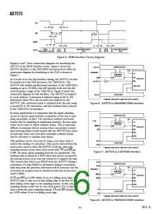
TIMING AND CONTROL OF THE AD7575
The two logic inputs on the AD7575, CS and RD, control both
the starting of conversion and the reading of data from the part.
A conversion is initiated by bringing both of these control inputs
LOW. Two interface options then exist for reading the output
data from the AD7575. These are the Slow Memory Interface
and ROM Interface, their operation is outlined below. It should
be noted that the TP pin of the AD7575 must be hard-wired
HIGH to ensure correct operation of the part. This pin is used
in testing the device and should not be used as a feedthrough pin
in double-sided printed circuit boards.
Faster versions of many processors, including the 8085A-2, test
the condition of the READY input very soon after the start of
an instruction cycle. Therefore, BUSY of the AD7575 must go
LOW very early in the cycle for the READY input to be effec-
tive in forcing the processor into a WAIT state. When using the
8085A-2, the processor S0 status signal provides the earliest
possible indication that a READ operation is about to occur.
Hence, S0 (which is LOW for a READ cycle) provides the
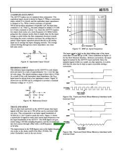
READ signal to the AD7575. The connection diagram for the
AD7575 to 8085A-2 Slow Memory interface is shown in
Figure 4.
SLOW MEMORY INTERFACE
The first interface option is intended for use with microproces-
sors that can be forced into a WAIT STATE for at least 5 µs.
The microprocessor (such as the 8085A) starts a conversion and
is halted until the result of the conversion is read from the con-
verter. Conversion is initiated by executing a memory READ to
the AD7575 address, bringing CS and RD LOW. BUSY subse-
quently goes LOW (forcing the microprocessor READY input
LOW), placing the processor into a WAIT state. The input
signal, which had been tracked by the analog input, is held on
the third falling clock edge of the input clock after CS and RD
have gone LOW (see Figure 12). The AD7575 then performs a
conversion on this acquired input signal value. When the con-
version is complete (BUSY goes HIGH), the processor com-
pletes the memory READ and acquires the newly converted
data. The timing diagram for this interface is shown in Figure 3.
ROM INTERFACE
The alternative interface option on the AD7575 avoids placing
the microprocessor into a WAIT state. In this interface, a con-
version is started with the first READ instruction, and the sec-
ond READ instruction accesses the data and starts a second
conversion. The timing diagram for this interface is shown in
Figure 5. It is possible to avoid starting another conversion on
the second READ (see below).
Conversion is initiated by executing a memory READ instruc-
tion to the AD7575 address, causing CS and RD to go LOW.
Data is also obtained from the AD7575 during this instruction.
This is old data and may be disregarded if not required. BUSY
goes LOW, indicating that conversion is in progress, and re-
turns HIGH when conversion is complete. Once again, the
input signal is held on the third falling edge of the input clock
after CS and RD have gone LOW.
A8–A15
ADDRESS BUS
+5V
TP
8085A–2
ADDRESS
DECODE
CS
The BUSY line may be used to generate an interrupt to the
microprocessor or monitored to indicate that conversion is
complete. The processor then reads the newly-converted data.
Alternatively, the delay between the convert start (first READ
instruction) and the data READ (second READ instruction)
must be at least as great as the AD7575 conversion time. For
the AD7575 to operate correctly in the ROM interface mode,
CS and RD should not go LOW before BUSY returns HIGH.
AD7575*
S0
RD
BUSY
ADDRESS
LATCH
ALE
DB0–DB7
AD0–AD7
READY
DATA BUS
Normally, the second READ instruction starts another conver-
sion as well as accessing the output data. However, if CS and
RD are brought LOW within one external clock period of
BUSY going HIGH, a second conversion does not occur.
*LINEAR CIRCUITRY OMITTED FOR CLARITY
SO = 0 FOR READ CYCLES
Figure 4. AD7575 to 8085A-2 Slow Memory Interface
REV. B
–5–

 ADI [ ADI ]