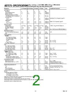
AD7575
CS
RD
t1
t5
t4
t8
t2
BUSY
t3
t3
t7
t7
HIGH
IMPEDANCE BUS
OLD
DATA
HIGH IMPEDANCE
BUS
NEW
DATA
HIGH IMPEDANCE
BUS
DATA
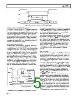
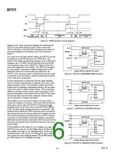
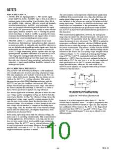
Figure 5. ROM Interface Timing Diagram
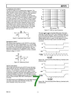
Figures 6 and 7 show connection diagrams for interfacing the
AD7575 in the ROM Interface mode. Figure 6 shows the
AD7575 interface to the 6502/6809 microprocessors while the
connection diagram for interfacing to the Z-80 is shown in
Figure 7.
ADDRESS BUS
A0–A15
+5V
6502/6809
TP
ADDRESS
DECODE
EN
R/W
CS
RD
AD7575*
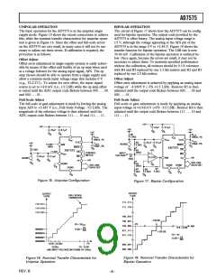
As a result of its very fast interface timing, the AD7575 can also
be interfaced to the DSP processor, the TMS32010. The
AD7575 will (within specifications) interface to the TMS32010,
running at up to 18 MHz, but will typically work over the full
clock frequency range of the TMS32010. Figure 8 shows the
connection diagram for this interface. The AD7575 is mapped
at a port address. Conversion is initiated using an IN A, PA
instruction where PA is the decoded port address for the
AD7575. The conversion result is obtained from the part using
a second IN A, PA instruction, and the resultant data is placed
in the TMS32010 accumulator.
2 OR E
DB0–DB7
DATA BUS
D0–D7
*LINEAR CIRCUITRY OMITTED FOR CLARITY
Figure 6. AD7575 to 6502/6809 ROM Interface
In many applications it is important that the signal sampling
occurs at exactly equal intervals to minimize errors due to sam-
pling uncertainty or jitter. The interfaces outlined previously
require that for sampling at equidistant intervals, the user must
count clock cycles or match software delays. This is especially
difficult in interrupt-driven systems where uncertainty in inter-
rupt servicing delays would require that the AD7575 have prior-
ity interrupt status and even then redundant software delays
may be necessary to equalize loop delays.
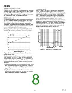
ADDRESS BUS
+5V
Z–80
TP
ADDRESS
DECODE
MREQ
RD
CS
EN
AD7575*
RD
DB7
DB0
DB7
DB0
This problem can be overcome by using a real time clock to
control the starting of conversion. This can be derived from the
clock source used to drive the AD7575 CLK pin. Since the
sampling instant occurs three clock cycles after CS and RD go
LOW, the input signal sampling intervals are equidistant. The
resultant data is placed in a FIFO latch that can be accessed by
the microprocessor at its own rate whenever it requires the data.
This ensures that data is not READ from the AD7575 during a
conversion. If a data READ is performed during a conversion,
valid data from the previous conversion will be accessed, but the
conversion in progress may be interfered with and an incorrect
result is likely.
DATA BUS
*LINEAR CIRCUITRY OMITTED FOR CLARITY
Figure 7. AD7575 to Z-80 ROM Interface
PA2
ADDRESS BUS
PA0
TMS32010
+5V
TP
ADDRESS
DECODE
MEN
DEN
EN
CS
AD7575*
If CS and RD go LOW within 20 ns of a falling clock edge, the
AD7575 may or may not see that falling edge as the first of the
three falling clock edges to the sampling instant. In this case, the
sampling instant could vary by one clock period. If it is impor-
tant to know the exact sampling instant, CS and RD should not
go LOW within 20 ns of a falling clock edge.
RD
DB7
DB0
D7
D0
DATA BUS
*LINEAR CIRCUITRY OMITTED FOR CLARITY
Figure 8. AD7575 to TMS32010 ROM Interface
REV. B
–6–

 ADI [ ADI ]