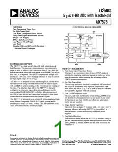
AD7575
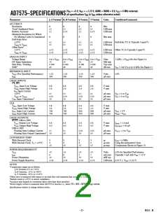
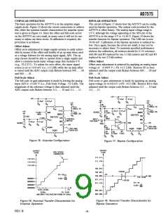
PIN CONFIGURATIONS
LCCC
DIP/SOIC
PLCC
1
2
3
4
5
6
7
8
9
18
17
16
15
14
13
12
11
10
V
V
CS
RD
TP
DD
2
3
1
20 19
3
2
1
20 19
REF
PIN 1
IDENTIFIER
AIN
4
5
6
7
8
18
17
16
15
14
18
4
5
6
7
8
AIN
TP
AIN
BUSY
AGND
DB0 (LSB)
DB1
CLK
17
16
15
AGND
DB0 (LSB)
DB1
AGND
DB0 (LSB)
DB1
BUSY
CLK
BUSY
CLK
AD7575
TOP VIEW
(Not to Scale)
AD7575
TOP VIEW
(Not to Scale)
AD7575
TOP VIEW
(Not to Scale)
DB7 (MSB)
DB6
DB7 (MSB)
DB6
DB7 (MSB)
DB6
14 DB2
DB5
DB2
DB2
9
10 11 12 13
DB5
DB3
9
10 11 12 13
DGND
DB4
NC = NO CONNECT
NC = NO CONNECT
ORDERING GUIDE
Relative
TERMINOLOGY
LEAST SIGNIFICANT BIT (LSB)
An ADC with 8-bits resolution can resolve 1 part in 28 (i.e.,
256) of full scale. For the AD7575 with +2.46 V full-scale one
LSB is 9.61 mV.
Temperature
Range
Accuracy
(LSB)
Package
Options2
Model1
AD7575JR
AD7575JN
AD7575KN
AD7575JP
AD7575KP
AD7575AQ
AD7575BQ
AD7575SQ
AD7575TQ
AD7575SE
AD7575TE
0°C to +70°C
0°C to +70°C
0°C to +70°C
0°C to +70°C
±1 max
±1 max
±1/2 max
±1 max
±1/2 max
±1 max
±1/2 max
±1 max
±1/2 max
±1 max
R-18
TOTAL UNADJUSTED ERROR
This is a comprehensive specification that includes full-scale
error, relative accuracy and offset error.
N-18
N-18
P-20A
P-20A
Q-18
Q-18
Q-18
Q-18
E-20A
E-20A
0°C to +70°C
RELATIVE ACCURACY
–25°C to +85°C
–25°C to +85°C
–55°C to +125°C
–55°C to +125°C
–55°C to +125°C
–55°C to +125°C
Relative Accuracy is the deviation of the ADC’s actual code
transition points from a straight line drawn between the devices
measured first LSB transition point and the measured full-scale
transition point.
±1/2 max
SNR
Signal-to-Noise Ratio (SNR) is the ratio of the desired signal to
the noise produced in the sampled and digitized analog signal.
SNR is dependent on the number of quantization levels used in
the digitization process; the more levels, the smaller the quantiza-
tion noise. The theoretical SNR for a sine wave input is given by
NOTES
1To order MIL-STD-883, Class B process parts, add /883B to part number.
Contact local sales office for military data sheet. For U.S. Standard Military
Drawing (SMD), see DESC drawing #5962-87762.
2E = Leadless Ceramic Chip Carrier; N = Plastic DIP; P = Plastic Leaded Chip
Carrier; Q = Cerdip, R = SOIC.
SNR = (6.02 N + 1.76) dB
where N is the number of bits in the ADC.
FULL-SCALE ERROR (GAIN ERROR)
The gain of a unipolar ADC is defined as the difference between
the analog input levels required to produce the first and the last
digital output code transitions. Gain error is a measure of the
deviation of the actual span from the ideal span of FS – 2 LSBs.
ANALOG INPUT RANGE
With VREF = +1.23 V, the maximum analog input voltage range
is 0 V to +2.46 V. The output data in LSBs is related to the
analog input voltage by the integer value of the following
expression:
256 AIN
2 VREF
Data (LSBs) =
+ 0.5
SLEW RATE
Slew Rate is the maximum allowable rate of change of input
signal such that the digital sample values are not in error. Slew
Rate limitations may restrict the analog signal bandwidth for
full-scale analog signals below the bandwidth allowed from
sampling theorem considerations.
REV. B
–4–

 ADI [ ADI ]