AD7575
INTERNAL/EXTERNAL CLOCK
EXTERNAL CLOCK
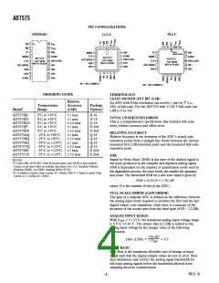
The AD7575 can be used with its own internal clock or with an
externally applied clock. In either case, the clock signal appear-
ing at the CLK pin is divided internally by two to provide an
internal clock signal for the AD7575. A single conversion lasts
for 20 input clock cycles (10 internal clock cycles).
The CLK input of the AD7575 may be driven directly from
74 HC, 4000B series buffers (such as 4049) or from LS TTL
with a 5.6 kΩ pull-up resistor. When conversion is complete, the
internal clock is disabled even if the external clock is still ap-
plied. This means that the external clock can continue to run
between conversions without being disabled. The mark/space
ratio of the external clock can vary from 70/30 to 30/70.
INTERNAL CLOCK
Clock pulses are generated by the action of the external capaci-
tor (CCLK) charging through an external resistor (RCLK) and
discharging through an internal switch. When a conversion is
complete, the internal clock stops operating. In addition to
conversion, the internal clock also controls the automatic inter-
nal reset of the SAR. This reset occurs at the start of each con-
version cycle during the first internal clock pulse.
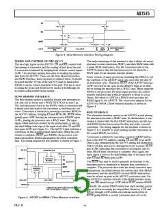
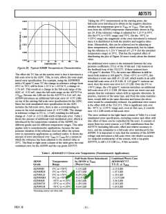
The AD7575 is specified for operation at a 5 µs conversion rate;
with a 4 MHz input clock frequency. If the part is operated at
slower clock frequencies, it may result in slightly degraded accu-
racy performance from the part. This is a result of leakage ef-
fects on the hold capacitor. Figure 14 shows a typical plot of
accuracy versus conversion time for the AD7575.
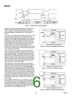
Nominal conversion times versus temperature for the recom-
mended RCLK and CCLK combination are shown in Figure 13.
2.5
T
= +25؇C
A
2.0
1.5
1.0
14
R
C
= 100k⍀
= 100pF
CLK
CLK
13
12
11
AD7575KN
10
0.5
0
9
8
7
5
10
50 100
500 1000
CONVERSION TIME – s
5000 10000
Figure 14. Accuracy vs. Conversion Time
–55
–25
0
+25
+50
+75
+100
+125
AMBIENT TEMPERATURE – ؇C
Figure 13. Typical Conversion Times vs. Temperature
Using Internal Clock
The internal clock is useful because it provides a convenient
clock source for the AD7575. Due to process variations, the
actual operating frequency for this RCLK/CCLK combination can
vary from device to device by up to ±50%. For this reason it is
recommended that an external clock be used in the following
situations:
1. Applications requiring a conversion time that is within 50% of
5 µs, the minimum conversion time for specified accuracy. A
clock frequency of 4 MHz at the CLK pin gives a conversion
time of 5 µs.
2. Applications where time related software constraints cannot
accommodate time differences that may occur due to unit to
unit clock frequency variations or temperature.
REV. B
–8–

 ADI [ ADI ]