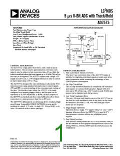
AD7575
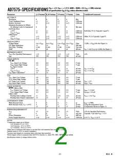
TIMING SPECIFICATIONS1 (VDD = +5 V, VREF = +1.23 V, AGND = DGND = 0 V)
Limit at +25؇C
(All Versions)
Limit at TMIN, TMAX
(J, K, A, B Versions)
Limit at TMIN, TMAX
(S, T Versions)
Parameter
Units
Conditions/Comments
t1
0
0
0
ns min
ns max
ns max
ns min
ns min
ns max
ns min
ns max
ns min
CS to RD Setup Time
RD to BUSY Propagation Delay
Data Access Time after RD
RD Pulse Width
CS to RD Hold Time
Data Access Time after BUSY
t22
100
100
100
0
80
10
80
0
100
100
100
0
80
10
80
0
120
120
120
0
100
10
t3
t4
t52
t63
t7
Data Hold Time
100
0
t8
BUSY to CS Delay
NOTES
1Timing specifications are sample tested at +25°C to ensure compliance. All input control signals are specified with tr = tf = 20 ns (10% to 90% of +5 V)
and timed from a voltage level of 1.6 V.
2t3 and t6 are measured with the load circuits of Figure 1 and defined as the time required for an output to cross 0.8 V or 2.4 V.
3t7 is defined as the time required for the data lines to change 0.5 V when loaded with the circuits of Figure 2.
Specifications subject to change without notice.
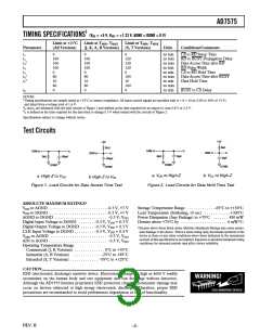
Test Circuits
+5V
3k⍀
+5V
3k⍀
DBN
DBN
DBN
DBN
3k⍀
10pF
3k⍀
100pF
10pF
100pF
DGND
DGND
DGND
DGND
a. VOH to High-Z
b. VOL to High-Z
a. High-Z to VOH
b High-Z to VOL
Figure 1. Load Circuits for Data Access Time Test
Figure 2. Load Circuits for Data Hold Time Test
ABSOLUTE MAXIMUM RATINGS*
VDD to AGND . . . . . . . . . . . . . . . . . . . . . . . . . . . –0.3 V, +7 V
Storage Temperature Range . . . . . . . . . . . . –65°C to +150°C
Lead Temperature (Soldering, 10 sec) . . . . . . . . . . . .+300°C
Power Dissipation (Any Package) to +75°C . . . . . . . 450 mW
Derates above +75°C by . . . . . . . . . . . . . . . . . . . . . 6 mW/°C
VDD to DGND . . . . . . . . . . . . . . . . . . . . . . . . . . . –0.3 V, +7 V
AGND to DGND . . . . . . . . . . . . . . . . . . . . . . . . –0.3 V, VDD
Digital Input Voltage to DGND . . . . . . . –0.3 V, VDD + 0.3 V
Digital Output Voltage to DGND . . . . . . –0.3 V, VDD + 0.3 V
CLK Input Voltage to DGND . . . . . . . . . –0.3 V, VDD + 0.3 V
VREF to AGND . . . . . . . . . . . . . . . . . . . . . . . . . . –0.3 V, VDD
AIN to AGND . . . . . . . . . . . . . . . . . . . . . . . . . . . –0.3 V, VDD
Operating Temperature Range
*Stresses above those listed under Absolute Maximum Ratings may cause perma-
nent damage to the device. This is a stress rating only; functional operation of the
device at these or any other conditions above those indicated in the operational
sections of this specification is not implied. Exposure to absolute maximum rating
conditions for extended periods may affect device reliability.
Commercial (J, K Versions) . . . . . . . . . . . . . . 0°C to +70°C
Industrial (A, B Versions) . . . . . . . . . . . . . –25°C to +85°C
Extended (S, T Versions) . . . . . . . . . . . . . –55°C to +125°C
CAUTION
ESD (electrostatic discharge) sensitive device. Electrostatic charges as high as 4000 V readily
accumulate on the human body and test equipment and can discharge without detection.
Although the AD7575 features proprietary ESD protection circuitry, permanent damage may
occur on devices subjected to high energy electrostatic discharges. Therefore, proper ESD
precautions are recommended to avoid performance degradation or loss of functionality.
WARNING!
ESD SENSITIVE DEVICE
REV. B
–3–

 ADI [ ADI ]