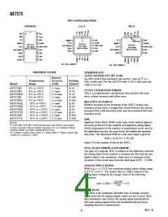
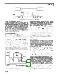
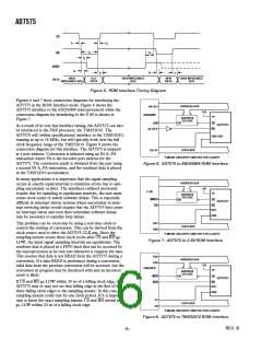
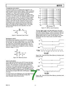
AD7575
UNIPOLAR OPERATION
BIPOLAR OPERATION
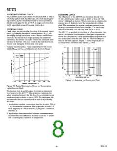
The basic operation for the AD7575 is in the unipolar single
supply mode. Figure 15 shows the circuit connections to achieve
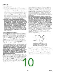
this, while the nominal transfer characteristic for unipolar opera-
tion is given in Figure 16. Since the offset and full-scale errors
on the AD7575 are very small, in many cases it will not be nec-
essary to adjust out these errors. If calibration is required, the
procedure is as follows:
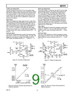
The circuit of Figure 17 shows how the AD7575 can be config-
ured for bipolar operation. The output code provided by the
AD7575 is offset binary. The analog input voltage range is
±5 V, although the voltage appearing at the AIN pin of the
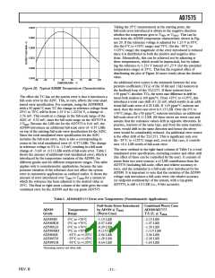
AD7575 is in the range 0 V to +2.46 V. Figure 18 shows the
transfer function for bipolar operation. The LSB size is now
39.06 mV. Calibration of the bipolar operation is outlined be-
low. Once again, because the errors are small, it may not be
necessary to adjust them. To maintain specified performance
without the calibration, all resistors should be 0.1% tolerance
with R4 and R5 replaced by one 3.3 kΩ resistor and R2 and R3
replaced by one 2.5 kΩ resistor.
Offset Adjust
Offset error adjustment in single-supply systems is easily achiev-
able by means of the offset null facility of an op amp when used
as a voltage follower for the analog input signal, AIN. The op
amp chosen should be able to operate from a single supply and
allow a common-mode input voltage range that includes 0 V
(e.g., TLC271). To adjust for zero offset, the input signal
source is set to +4.8 mV (i.e., 1/2 LSB) while the op amp offset
is varied until the ADC output code flickers between 000 . . . 00
and 000 . . . 01.
Offset Adjust
Offset error adjustment is achieved by applying an analog input
voltage of –4.9805 V (–FS +1/2 LSB). Resistor R3 is then
adjusted until the output code flickers between 000 . . . 00 and
000 . . . 01.
Full-Scale Adjust
Full-Scale Adjust
The full scale or gain adjustment is made by forcing the analog
input AIN to +2.445 V (i.e., Full-Scale Voltage –3/2 LSB). The
magnitude of the reference voltage is then adjusted until the
ADC output code flickers between 111 . . . 10 and 111. . . 11.
Full-scale or gain adjustment is made by applying an analog
input voltage of +4.9414 V (+FS –3/2 LSB). Resistor R4 is then
adjusted until the output code flickers between 111 . . . 10 and
111. . . 11.
+5V
+
+5V
47F
0.1F
+5V
47F
0.1F
+5V
A
A
+5V
A
A
R
CLK
R8
3.3k⍀
R
100k⍀, 1%
CLK
V
DD
100k⍀, 1%
V
CLK
V
REF
DD
C
+
CLK
CLK
47F
0.1F
R2
2.2k⍀
+5V
3.3k⍀
C
100pF, 2%
CLK
AD589
+2.46V
MAX
AIN
BUSY
100pF, 2%
D
–
D
A
A
BUSY
AD7575
CS
RD
TP
A
R3
500⍀
+5V
AD7575
+1.23V
0.1F
CS
RD
TP
CONTROL
INPUT
VOLTAGE
V
REF
+
INPUTS
47F
R1
10k⍀
TLC271
A
AIN
+5V
AD589
+5V
–
A
A
DB7–DB0
DATA OUT
A
R4
500⍀
AGND
AGND
DGND
DB7–DB0
DATA OUT
A
DGND
R7
2.5k⍀
R5
3k⍀
R6
2.5k⍀
A
D
D
A
A
Figure 15. Unipolar Configuration
Figure 17. Bipolar Configuration
OUTPUT
CODE
OUTPUT
FULL SCALE
CODE
TRANSITION
111...111
11111111
11111110
11111101
111...110
100...010
100...001
100...000
011...111
011...110
–1/2LSB
–FS
FS = 2V
1LSB =
REF
AIN
+FS –1LSB
FS
256
00000011
00000010
+1/2LSB
FS = 5V
FS
256
00000001
00000000
1LSB =
1LSB 3LSBs
2LSBs
FS
FS –1LSB
000...001
000...000
AIN, INPUT VOLTAGE (IN TERMS OF LSBs)
Figure 16. Nominal Transfer Characteristic for
Unipolar Operation
Figure 18. Nominal Transfer Characteristic for
Bipolar Operation
REV. B
–9–

 ADI [ ADI ]