AD650
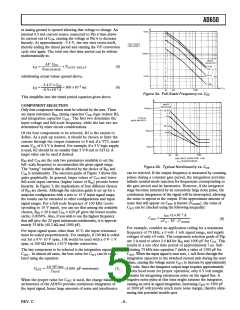
scale, if the maximum frequency error is 5 Hz, the nonlinearity
would be specified as 50 ppm or 0.005%. Typically on the
100 kHz scale, the nonlinearity is positive and the maximum
value occurs at about midscale (Figure 9a). At higher full-scale fre-
quencies, (500 kHz to 1 MHz), the nonlinearity becomes “S”
shaped and the maximum value may be either positive or nega-
tive. Typically, on the 1 MHz scale (RIN = 16.9k, COS = 51 pF)
the nonlinearity is positive below about 2/3 scale and is negative
above this point. This is shown graphically in Figure 9b.
in the figure will never call for a negative voltage at the output
but one may imagine an arrangement calling for a bipolar out-
put voltage (say 10 volts) by connecting an extra resistor from
Pin 3 to a positive voltage. This will not work.
Care should be taken under conditions where a high positive
input voltage exists at or before power up. These situations can
cause a latch up at the integrator output (Pin 1). This is a non-
destructive latch and, as such, normal operation can be restored
by cycling the power supply. Latch up can be prevented by
connecting two diodes (e.g., 1N914 or 1N4148) as shown in
Figure 4, thereby, preventing Pin 1 from swinging below Pin 2.
PSRR
The power supply rejection ratio is a specification of the change
in gain of the AD650 as the power supply voltage is changed.
The PSRR is expressed in units of parts-per-million change of
the gain per percent change of the power supply—ppm/%. For
example, consider a VFC with a 10 volt input applied and an
output frequency of exactly 100 kHz when the power supply
potential is 15 volts. Changing the power supply to 12.5 volts
is a 5 volt change out of 30 volts, or 16.7%. If the output frequency
changes to 99.9 kHz, the gain has changed 0.1% or 1000 ppm.
The PSRR is 1000 ppm divided by 16.7% which equals 60 ppm/%.
A second major difference is that the output will only sink 1 mA
to the negative supply. There is no pulldown stage at the output
other than the 1 mA current source used for the V-to-F conver-
sion. The op amp will source a great deal of current from the
positive supply, and it is internally protected by current limiting.
The output of the op amp may be driven to within 3 volts of the
positive supply when it is not sourcing external current. When
sourcing 10 mA the output voltage may be driven to within
6 volts of the positive supply.
A third difference between this op amp and a normal device is
that the inverting input, Pin 3, is bias current compensated and
the noninverting input is not bias current compensated. The
bias current at the inverting input is nominally zero, but may be
as much as 20 nA in either direction. The noninverting input
typically has a bias current of 40 nA that always flows into the
node (an npn input transistor). Therefore, it is not possible to
match input voltage drops due to bias currents by matching
input resistors.
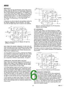
The PSRR of the AD650 is a function of the full-scale operating
frequency. At low full-scale frequencies the PSRR is determined
by the stability of the reference circuits in the device and can be
very good. At higher frequencies there are dynamic errors which
become more important than the static reference signals, and
consequently the PSRR is not quite as good. The values of PSRR
are typically 0
= 40 k, COS = 3300 pF). At 100 kHz (RIN = 40k, COS = 330 pF)
the PSRR is typically +80 40 ppm/%, and at 1 MHz (RIN
20 ppm/% at 10 kHz full-scale frequency (RIN
=
The op amp has provisions for trimming the input offset volt-
age. A potentiometer of 20 kΩ is connected to Pins 13 and 14
and the wiper is connected to the positive supply through a
250 kΩ resistor. A potential of about 0.6 volt is established
across the 250 kΩ resistor, and the 3 µA current is injected into
the null pins. It is also possible to null the op amp offset voltage
by using only one of the null pins and use a bipolar current
either into or out of the null pin. The amount of current required
will be very small—typically less than 3 µA. This technique is
shown in the applications section of this data sheet: the autozero
circuit uses this technique.
16.9 kΩ, COS = 51 pF) the PSRR is +350 50 ppm/%. This
information is summarized graphically in Figure 10.
The bipolar offset current is activated by connecting a 1.24 kΩ
resistor between Pin 4 and the negative supply. The resultant
current delivered to the op amp noninverting input is nominally
0.5 mA and has a tolerance of 10%. This current is then used
to provide an offset voltage when Pin 2 is tied to ground through a
resistor. The 0.5 mA which appears at Pin 2 is also flowing through
the 1.24 kΩ resistor and this current may be by observing the
voltage across the 1.24 kΩ resistor. An external resistor is used
to activate the bipolar offset current source to provide the lowest
tolerance and temperature drift of the resultant offset voltage. It
is possible to use other values of resistance between Pin 4 and –VS
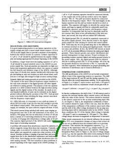
to obtain a bipolar offset current different than 0.5 mA. Fig-
ure 11 is a graph of the relationship between the bipolar offset
current and the value of the resistor used to activate the source.
Figure 10. PSRR vs. Full-Scale Frequency
OTHER CIRCUIT CONSIDERATIONS
The input amplifier connected to Pins 1, 2 and 3 is not a standard
operational amplifier. Rather, the design has been optimized for
simplicity and high speed. The single largest difference between
this amplifier and a normal op amp is the lack of an integrator
(or level shift) stage. Consequently the voltage on the output
(Pin 1) must always be more positive than 2 volts below the
inputs (Pins 2 and 3). For example, in the F-to-V conversion
mode, see Figure 6, the noninverting input of the op amp (Pin 2) is
grounded, which means that the output (Pin 1) will not be able
to go below –2 volts. Normal operation of the circuit as shown
REV. C
–9–

 ADI [ ADI ]