AD650
at analog ground is opened allowing that voltage to change. An
internal 0.5 mA current source connected to Pin 6 then draws
its current out of COS, causing the voltage at Pin 6 to decrease
linearly. At approximately –3.4 V, the one shot resets itself,
thereby ending the timed period and starting the V/F conversion
cycle over again. The total one shot time period can be written
mathematically as:
∆V COS
IDISCHARGE
tOS
=
+TGATE DELAY
(5)
substituting actual values quoted above,
–3.4V × COS
tOS
=
+ 300 ×10–9 sec
(6)
–0.5 ×10⁻³
A
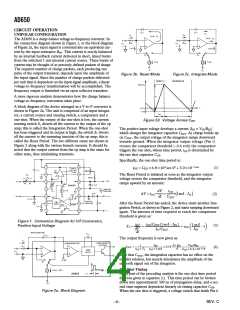
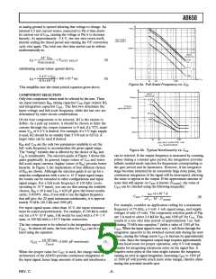
Figure 3a. Full-Scale Frequency vs. COS
This simplifies into the timed period equation given above.
COMPONENT SELECTION
Only four component values must be selected by the user. These
are input resistance RIN, timing capacitor COS, logic resistor R2,
and integration capacitor CINT. The first two determine the
input voltage and full-scale frequency, while the last two are
determined by other circuit considerations.
Of the four components to be selected, R2 is the easiest to
define. As a pull-up resistor, it should be chosen to limit the
current through the output transistor to 8 mA if a TTL maxi-
mum VOL of 0.4 V is desired. For example, if a 5 V logic supply
is used, R2 should be no smaller than 5 V/8 mA or 625 Ω. A
larger value can be used if desired.
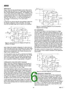
RIN and COS are the only two parameters available to set the
full- scale frequency to accommodate the given signal range.
The “swing” variable that is affected by the choice of RIN and
Figure 3b. Typical Nonlinearity vs. COS
can be rejected. If the output frequency is measured by counting
pulses during a constant gate period, the integration provides
infinite normal-mode rejection for frequencies corresponding to
the gate period and its harmonics. However, if the integrator
stage becomes saturated by an excessively large noise pulse, the
continuous integration of the signal will be interrupted, allowing
the noise to appear at the output. If the approximate amount of
noise that will appear on CINT is known (VNOISE), the value of
CINT can be checked using the following inequality:
C
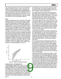
OS is nonlinearity. The selection guide of Figure 3 shows this
quite graphically. In general, larger values of COS and lower
full-scale input currents (higher values of RIN) provide better
linearity. In Figure 3, the implications of four different choices
of RIN are shown. Although the selection guide is set up for a
unipolar configuration with a zero to 10 V input signal range,
the results can be extended to other configurations and input
signal ranges. For a full scale frequency of 100 kHz (corre-
sponding to 10 V input), you can see that among the available
choices, RIN = 20 k and COS = 620 pF gives the lowest nonlin-
earity, 0.0038%. Also, if you wish to use the highest frequency
that will give the 20 ppm minimum nonlinearity, it is approxi-
mately 33 kHz (40.2 kΩ and 1000 pF).
tOS ×1×10⁻³
+VS – 3V –VNOISE
A
CINT
>
(8)
For example, consider an application calling for a maximum
frequency of 75 kHz, a 0 volt–1 volt signal range, and supply
voltages of only 9 volts. The component selection guide of Fig-
ure 3 is used to select 2.0 kΩ for RIN and 1000 pF for COS. This
results in a one shot time period of approximately 7 µs. Sub-
stituting 75 kHz into equation 7 yields a value of 1300 pF for
CINT. When the input signal is near zero, 1 mA flows through the
integration capacitor to the switched current sink during the reset
phase, causing the voltage across CINT to increase by approximately
5.5 volts. Since the integrator output stage requires approximately
3 volts head room for proper operation, only 0.5 volt margin
remains for integrating extraneous noise on the signal line. A
negative noise pulse at this time might saturate the integrator,
causing an error in signal integration. Increasing CINT to 1500 pF
or 2000 pF will provide much more noise margin, thereby elimi-
nating this potential trouble spot.
For input signal spans other than 10 V, the input resistance
must be scaled proportionately. For example, if 100 kΩ is called
out for a 0 V–10 V span, 10k would be used with a 0 V–1 V
span, or 200 kΩ with a 10 V bipolar connection.
The last component to be selected is the integration capacitor
C
INT. In almost all cases, the best value for CINT can be calcu-
lated using the equation:
10–4F/sec
CINT
=
(1000 pF minimum)
(7)
fMAX
When the proper value for CINT is used, the charge balance
architecture of the AD650 provides continuous integration of
the input signal, hence large amounts of noise and interference
REV. C
–5–

 ADI [ ADI ]