AD650
constant offset voltage will not affect dynamic range but simply
shift all of the frequency readings by a few hertz. However, if the
offset should change, then it will not be possible to distinguish
between a small change in a small input voltage and a drift of
the offset voltage. Hence, the usable dynamic range is less. The
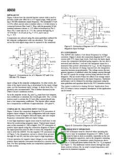
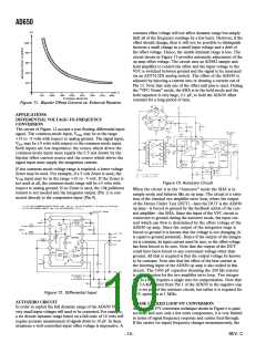
circuit shown in Figure 13 provides automatic adjustment of the
op amp offset voltage. The circuit uses an AD582 sample and
hold amplifier to control the offset and the input voltage to the
VFC is switched between ground and the signal to be measured
via an AD7512DI analog switch. The offset of the AD650 is
adjusted by injecting a current into or drawing a current out of
Pin 13. Note that only one of the offset null pins is used. During
the “VFC Norm” mode, the SHA is in the hold mode and the
hold capacitor is very large, 0.1 µF, to hold the AD650 offset
constant for a long period of time.
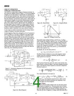
Figure 11. Bipolar Offset Current vs. External Resistor
APPLICATIONS
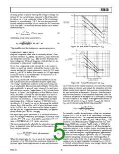
DIFFERENTIAL VOLTAGE-TO-FREQUENCY
CONVERSION
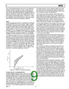
The circuit of Figure 12 accepts a true floating differential input
signal. The common-mode input, VCM, may be in the range
+15 to –5 volts with respect to analog ground. The signal input,
VIN, may be 5 volts with respect to the common-mode input.
Both inputs are low impedance: the source which drives the
common-mode input must supply the 0.5 mA drawn by the
bipolar offset current source and the source which drives the
signal input must supply the integration current.
If less common-mode voltage range is required, a lower voltage
Zener may be used. For example, if a 5 volt Zener is used, the
V
CM input may be in the range +10 to –5 volt. If the Zener is
Figure 13. Autozero Circuit
not used at all, the common-mode range will be 5 volts with
respect to analog ground. If no Zener is used, the 10k pulldown
resistor is not needed and the integrator output (Pin 1) is con-
nected directly to the comparator input (Pin 9).
When the circuit is in the “Autozero” mode the SHA is in
sample mode and behaves like an op amp. The circuit is a varia-
tion of the classical two amplifier servo loop, where the output
of the Device Under Test (DUT)—here the DUT is the AD650
op amp—is forced to ground by the feedback action of the con-
trol amplifier—the SHA. Since the input of the VFC circuit is
connected to ground during the autozero mode, the input cur-
rent which can flow is determined by the offset voltage of the
AD650 op amp. Since the output of the integrator stage is
forced to ground it is known that the voltage is not changing (it
is equal to ground potential). Hence if the output of the integra-
tor is constant, its input current must be zero, so the offset voltage
has been forced to be zero. Note that the output of the DUT
could have been forced to any convenient voltage other than
ground. All that is required is that the output voltage be known
to be constant. Note also that the effect of the bias current at
the inverting input of the AD650 op amp is also nulled in this
circuit. The 1000 pF capacitor shunting the 200 kΩ resistor
is compensation for the two amplifier servo loop. Two integra-
tors in a loop requires a single zero for compensation. Note that
the 3.6 kΩ resistor from Pin 1 of the AD650 to the negative sup-
ply is not part of the autozero circuit, but rather it is required for
VFC operation at 1 MHz.
Figure 12. Differential Input
AUTOZERO CIRCUIT
PHASE LOCKED LOOP F/V CONVERSION
In order to exploit the full dynamic range of the AD650 VFC,
very small input voltages will need to be converted. For example,
a six decade dynamic range based on a full scale of 10 volts will
require accurate measurement of signals down to 10 µV. In these
situations a well-controlled input offset voltage is imperative. A
Although the F/V conversion technique shown in Figure 6 is quite
accurate and uses only a few extra components, it is very limited
in terms of signal frequency response and carrier feed-through.
If the carrier (or input) frequency changes instantaneously, the
–10–
REV. C

 ADI [ ADI ]