AD650
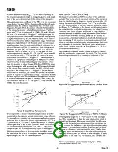
by either drift or tolerance of CINT. The net effect of a change in
the integrator capacitor is simply to change the peak to peak ampli-
tude of the sawtooth waveform at the output of the integrator.
NONLINEARITY SPECIFICATION
The linearity error of the AD650 is specified by the endpoint
method. That is, the error is expressed in terms of the deviation
from the ideal voltage to frequency transfer relation after cali-
brating the converter at full scale and “zero”. The nonlinearity
will vary with the choice of one-shot capacitor and input resistor
(see Figure 3). Verification of the linearity specification requires
the availability of a switchable voltage source (or a DAC) having
a linearity error below 20 ppm, and the use of very long mea-
surement intervals to minimize count uncertainties. Every AD650
is automatically tested for linearity, and it will not usually be
necessary to perform this verification, which is both tedious and
time consuming. If it is required to perform a nonlinearity test
either as part of an incoming quality screening or as a final prod-
uct evaluation, an automated “bench-top” tester would prove
useful. Such a system based on the Analog Devices’ LTS-2010
is described in Reference 2.
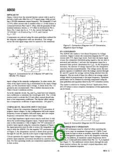
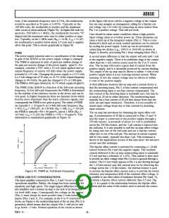
The gain temperature coefficient of the AD650 is not a constant
value. Rather the gain TC is a function of both the full-scale
frequency and the ambient temperature. At a low full-scale
frequency, the gain TC is determined primarily by the stability
of the internal reference—a buried Zener reference. This low
speed gain TC can be quite good; at 10 kHz full scale, the gain
TC near 25°C is typically 0 50 ppm/°C. Although the gain TC
changes with ambient temperature (tending to be more positive
at higher temperatures), the drift remains within a 75 ppm/°C
window over the entire military temperature range. At full-scale
frequencies higher than 10 kHz dynamic errors become much
more important than the static drift of the dc reference. At a
full-scale frequency of 100 kHz and above, these timing errors
dominate the gain TC. For example, at 100 kHz full-scale
frequency (RIN = 40 k and COS = 330 pF) the gain TC near
room temperature is typically –80 50 ppm/°C, but at an ambi-
ent temperature near +125°C, the gain TC tends to be more
positive and is typically +15 50 ppm/°C. This information is
presented in a graphical form in Figure 8. The gain TC always
tends to become more positive at higher temperatures. There-
fore, it is possible to adjust the gain TC of the AD650 by using
a one-shot capacitor with an appropriate TC to cancel the drift
of the circuit. For example, consider the 100 kHz full-scale
frequency. An average drift of –100 ppm/°C means that as
temperature is increased, the circuit will produce a lower fre-
quency in response to a given input voltage. This means that the
one-shot capacitor must decrease in value as temperature increases
in order to compensate the gain TC of the AD650; that is, the
capacitor must have a TC of –100 ppm/°C. Now consider the
1 MHz full-scale frequency.
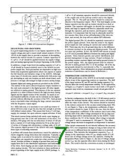
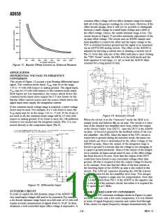
The voltage-to-frequency transfer relation is shown in Figure 9
with the nonlinearity exaggerated for clarity. The first step in
determining nonlinearity is to connect the endpoints of the
Figure 9a. Exaggerated Nonlinearity at 100 kHz Full Scale
Figure 8. Gain TC vs. Temperature
It is not possible to achieve very much improvement in perfor-
mance unless the expected ambient temperature range is known.
For example, in a constant low temperature application such as
gathering data in an Arctic climate (approximately –20°C), a
COS with a drift of –310 ppm/°C is called for in order to compen-
sate the gain drift of the AD650. However, if that circuit should
see an ambient temperature of +75°C, the COS cap would
change the gain TC from approximately 0 ppm to +310 ppm/°C.
Figure 9b. Exaggerated Nonlinearity at 1 MHz Full Scale
operating range (typically at 10 mV and 10 V) with a straight
line. This straight line is then the ideal relationship which is
desired from the circuit. The second step is to find the difference
between this line and the actual response of the circuit at a few
points between the endpoints—typically ten intermediate points
will suffice. The difference between the actual and the ideal
response is a frequency error measured in hertz. Finally, these
frequency errors are normalized to the full-scale frequency and
expressed either as parts per million of full scale (ppm) or parts
per hundred of full scale (%). For example, on a 100 kHz full
The temperature effects of the components described above are
the same when the AD650 is configured for negative or bipolar
input voltages, and for F/V conversion as well.
2“V–F Converters Demand Accurate Linearity Testing,” by L. DeVito,
(Electronic Design, March 4, 1982).
–8–
REV. C

 ADI [ ADI ]