AD650
BIPOLAR V/F
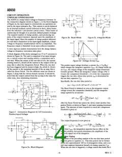
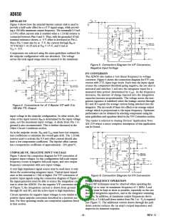
Figure 4 shows how the internal bipolar current sink is used to
provide a half-scale offset for a 5 V signal range, while provid-
ing a 100 kHz maximum output frequency. The nominally 0.5 mA
( 10%) offset current sink is enabled when a 1.24 kΩ resistor is
connected between Pins 4 and 5. Thus, with the grounded 10 kΩ
nominal resistance shown, a –5 V offset is developed at Pin 2.
Since Pin 3 must also be at –5 V, the current through RIN is
10 V/40 kΩ = +0.25 mA at VIN = +5 V, and 0 mA at
VIN = –5 V.
Components are selected using the same guidelines outlined for
the unipolar configuration with one alteration. The voltage
across the total signal range must be equated to the maximum
Figure 5. Connection Diagram for V/F Conversion,
Negative Input Voltage
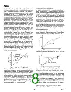
F/V CONVERSION
The AD650 also makes a very linear frequency-to-voltage
converter. Figure 6 shows the connection diagram for F/V con-
version with TTL input logic levels. Each time the input signal
crosses the comparator threshold going negative, the one shot is
activated and switches 1 mA into the integrator input for a
measured time period (determined by COS). As the frequency
increases, the amount of charge injected into the integration
capacitor increase proportionately. The voltage across the inte-
gration capacitor is stabilized when the leakage current through
R1 and R3 equals the average current being switched into the
integrator. The net result of these two effects is an average output
voltage which is proportional to the input frequency. Optimum
performance can be obtained by selecting components using the
same guidelines and equations listed in the V/F Conversion section.
Figure 4. Connections for 5 V Bipolar V/F with 0 to
100 kHz TTL Output
input voltage in the unipolar configuration. In other words, the
value of the input resistor RIN is determined by the input voltage
span, not the maximum input voltage. A diode from Pin 1 to
ground is also recommended. This is further discussed in the
Other Circuit Conditions section.
The reader is referred to Analog Devices' Application Note
AN-279 where a more complete description of this application
can be found.
As in the unipolar circuit, RIN and COS must have low tempera-
ture coefficients to minimize the overall gain drift. The 1.24 kΩ
resistor used to activate the 0.5 mA offset current should also
have a low temperature coefficient. The bipolar offset current
has a temperature coefficient of approximately –200 ppm/°C.
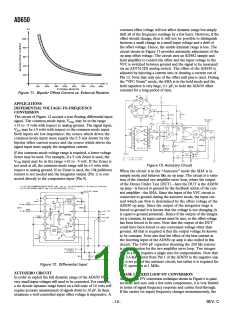
UNIPOLAR V/F, NEGATIVE INPUT VOLTAGE
Figure 5 shows the connection diagram for V/F conversion of
negative input voltages. In this configuration full-scale output
frequency occurs at negative full-scale input, and zero output
frequency corresponds with zero input voltage.
A very high impedance signal source may be used since it only
drives the noninverting integrator input. Typical input imped-
ance at this terminal is 1 GΩ or higher. For V/F conversion of
positive input signals using the connection diagram of Figure 1,
the signal generator must be able to source the integration cur-
rent to drive the AD650. For the negative V/F conversion circuit
of Figure 5, the integration current is drawn from ground
through R1 and R3, and the active input is high impedance.
Figure 6. Connection Diagram for F/V Conversion
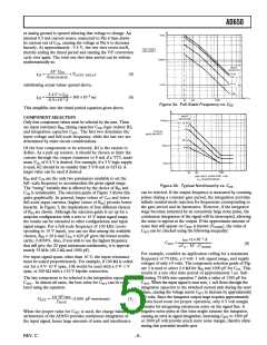
HIGH FREQUENCY OPERATION
Proper RF techniques must be observed when operating the
AD650 at or near its maximum frequency of 1 MHz. Lead
lengths must be kept as short as possible, especially on the one
shot and integration capacitors, and at the integrator summing
junction. In addition, at maximum output frequencies above
500 kHz, a 3.6 kΩ pull-down resistor from Pin 1 to –VS is required
(see Figure 7). The additional current drawn through the pull-
down resistor reduces the op amp’s output impedance and
improves its transient response.
Circuit operation for negative input voltages is very similar to
positive input unipolar conversion described in a previous sec-
tion. For best operating results use component equations listed
in that section.
–6–
REV. C

 ADI [ ADI ]