AD650
1 µF to 10 µF tantalum capacitor should be connected directly
to the supply side of the pull-up resistor and to the digital
ground—Pin 10. The pull-up resistor should be connected
directly to the frequency output—Pin 8. The lead lengths on the
bypass capacitor and the pull up resistor should be as short as
possible. The capacitor will supply (or absorb) the current tran-
sients, and large ac signals will flow in a physically small loop
through the capacitor, pull up resistor, and frequency output
transistor. It is important that the loop be physically small for
two reasons: first, there is less self-inductance if the wires are
short, and second, the loop will not radiate RFI efficiently.
The digital ground (Pin 10) should be separately connected to
the power supply ground. Note that the leads to the digital
power supply are only carrying dc current and cannot radiate
RFI. There may also be a dc ground drop due to the difference
in currents returned on the analog and digital grounds. This will
not cause any problem. In fact, the AD650 will tolerate as much
as 0.25 volt dc potential difference between the analog and digital
grounds. These features greatly ease power distribution and
ground management in large systems. Proper technique for
grounding requires separate digital and analog ground returns to
the power supply. Also, the signal ground must be referred
directly to analog ground (Pin 11) at the package. All of the sig-
nal grounds should be tied directly to Pin 11, especially the
one-shot capacitor. More information on proper grounding and
reduction of interference can be found in Reference 1.
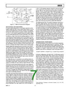
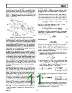
Figure 7. 1 MHz V/F Connection Diagram
DECOUPLING AND GROUNDING
It is good engineering practice to use bypass capacitors on the
supply-voltage pins and to insert small-valued resistors (10 Ω to
100 Ω) in the supply lines to provide a measure of decoupling
between the various circuits in a system. Ceramic capacitors of
0.1 µF to 1.0 µF should be applied between the supply-voltage
pins and analog signal ground for proper bypassing on the AD650.
In addition, a larger board level decoupling capacitor of 1 µF to
10 µF should be located relatively close to the AD650 on each
power supply line. Such precautions are imperative in high reso-
lution data acquisition applications where one expects to exploit
the full linearity and dynamic range of the AD650. Although
some types of circuits may operate satisfactorily with power sup-
ply decoupling at only one location on each circuit board, such
practice is strongly discouraged in high accuracy analog design.
TEMPERATURE COEFFICIENTS
The drift specifications of the AD650 do not include temperature
effects of any of the supporting resistors or capacitors. The drift
of the input resistors R1 and R3 and the timing capacitor COS
directly affect the overall temperature stability. In the application
of Figure 2, a 10 ppm/°C input resistor used with a 100 ppm/°C
capacitor may result in a maximum overall circuit gain drift of:
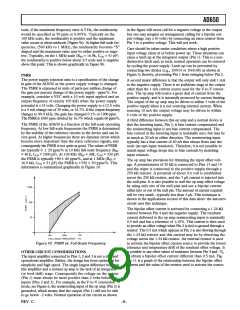
Separate digital and analog grounds are provided on the AD650.
The emitter of the open collector frequency output transistor is
the only node returned to the digital ground. All other signals
are referred to analog ground. The purpose of the two separate
grounds is to allow isolation between the high precision analog
signals and the digital section of the circuitry. As much as sev-
eral hundred millivolts of noise can be tolerated on the digital
ground without affecting the accuracy of the VFC. Such ground
noise is inevitable when switching the large currents associated
with the frequency output signal.
150 ppm/°C (AD650A) + 100 ppm/°C (COS) + 10 ppm/°C (RIN) 260 ppm/°C
In bipolar configuration, the drift of the 1.24 kΩ resistor used to
activate the internal bipolar offset current source will directly
affect the value of this current. This resistor should be matched
to the resistor connected to the op amp noninverting input (Pin
2), see Figure 4. That is, the temperature coefficients of these
two resistors should be equal. If this is the case, then the effects
of the temperature coefficients of the resistors cancel each other,
and the drift of the offset voltage developed at the op amp non-
inverting input will be determined solely by the AD650. Under
these conditions the TC of the bipolar offset voltage is typically
–200 ppm/°C and is a maximum of –300 ppm/°C. The offset
voltage always decreases in magnitude as temperature is increased.
At 1 MHz full scale, it is necessary to use a pull-up resistor of
about 500 Ω in order to get the rise time fast enough to provide
well defined output pulses. This means that from a 5 volt logic
supply, for example, the open collector output will draw 10 mA.
This much current being switched will surely cause ringing on
long ground runs due to the self inductance of the wires. For
instance, #20 gauge wire has an inductance of about 20 nH per
inch; a current of 10 mA being switched in 50 ns at the end of
12 inches of 20 gauge wire will produce a voltage spike of 50 mV.
The separate digital ground of the AD650 will easily handle
these types of switching transients.
Other circuit components do not directly influence the accuracy
of the VFC over temperature changes as long as their actual val-
ues are not so different from the nominal value as to preclude
operation. This includes the integration capacitor, CINT. A
change in the capacitance value of CINT simply results in a dif-
ferent rate of voltage change across the capacitor. During the
Integration Phase (refer to Figure 2), the rate of voltage change
across CINT has the opposite effect that it does during the Reset
Phase. The result is that the conversion accuracy is unchanged
A problem will remain from interference caused by radiation of
electro-magnetic energy from these fast transients. Typically, a
voltage spike is produced by inductive switching transients;
these spikes can capacitively couple into other sections of the
circuit. Another problem is ringing of ground lines and power
supply lines due to the distributed capacitance and inductance
of the wires. Such ringing can also couple interference into sen-
sitive analog circuits. The best solution to these problems is
proper bypassing of the logic supply at the AD650 package. A
1“Noise Reduction Techniques in Electronic Systems,” by H. W. OTT,
(John Wiley, 1976).
REV. C
–7–

 ADI [ ADI ]