AD650
output cannot change very rapidly due to the integrator time
constant formed by CINT and RIN. While it is possible to decrease
the integrator time constant to provide faster settling of the
F-to-V output voltage, the carrier feedthrough will then be
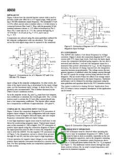
larger. For signal frequency response in excess of 2 kHz, a phase
locked F/V conversion technique such as the one shown in Fig-
ure 14 is recommended.
the AD650 slightly, driving the system towards synchronization.
In a similar manner, if the input carrier lags the output carrier,
the integrator will be forced down slightly to synchronize the
two signals.
Using a mathematical approach, the 25 µA pulses from the
phase detector are incorporated into the phase detector gain, Kd.
Using a mathematical approach, the 25 µA pulses from the
phase detector are incorporated into the phase detector gain, Kd.
25 µA
2π
Kd =
= 4 ×10⁻⁶ amperes/radian
(9)
Also, the V/F converter is configured to produce 1 MHz in
response to a 10 volt input, so its gain Ko, is:
2 π ×1×106 Hz
radians
volt • sec
Ko =
= 6.3 ×10⁵
(10)
10V
The dynamics of the phase relationship between the input and
output signals can be characterized as a second order system
with natural frequency ωn:
KoKd
C
(11)
ωn =
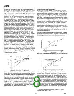
Figure 14. Phase Locked Loop F/V Conversion
In a phase locked loop circuit, the oscillator is driven to a frequency
and phase equal to an input reference signal. In applications
such as a synthesizer, the oscillator output frequency is first pro-
cessed through a programmable “divide by N” before being
applied to the phase detector as feedback. Here the oscillator
frequency is forced to be equal to “N times” the reference fre-
quency and it is this frequency output which is the desired
output signal and not a voltage. In this case, the AD650 offers
compact size and wide dynamic range.
and damping factor
R C KoKd
(12)
ζ =
2
For the values shown in Figure 14, these relations simplify to a
natural frequency of 35 kHz with a damping factor of 0.8.
For those desiring a simple approach to determining component
values for other PLL frequencies and VFC full-scale voltage, the
following cookbook steps can be used:
In signal recovery applications of a PLL, the desired output sig-
nal is the voltage applied to the oscillator. In these situations a
linear relationship between the input frequency and the output
voltage is desired; the AD650 makes a superb oscillator for FM
demodulation. The wide dynamic range and outstanding linearity
of the AD650 VFC allow simple embodiment of high perfor-
mance analog signal isolation or telemetry systems. The circuit
shown in Figure 14 uses a digital phase detector which also pro-
vides proper feedback in the event of unequal frequencies. Such
phase-frequency detectors (PFDs) are available in integrated
form. For a full discussion of phase lock loop circuits see
Reference 3.
1. Determine Ko (in units of radians per volt second) from the
maximum input carrier frequency FMAX (in hertz) and the
maximum output voltage VMAX
.
2 π × FMAX
Ko =
(13)
VMAX
2. Calculate a value for C based upon the desired loop band-
width, fn. Note that this is the desired frequency range of the
output signal. The loop bandwidth (fn) is not the maximum
carrier frequency (fMAX): the signal may be very narrow even
though it is transmitted over a 1 MHz carrier.
An analysis of this circuit must begin at the 7474 dual D flip
flop. When the input carrier matches the output carrier in both
phase and frequency, the Q outputs of the flip flops will rise at
exactly the same time. With two zeros, then two ones on the
inputs of the exclusive or (XOR) gate, the output will remain
low keeping the DMOS FET switched off. Also, the NAND
gate will go low resetting the flip-flops to zero. Throughout the
entire cycle just described, the DMOS integrator gate remained
off, allowing the voltage at the integrator output to remain
unchanged from the previous cycle. However, if the input carrier
leads the output carrier by a few degrees, the XOR gate will be
turned on for the small time span that the two signals are mis-
matched. Since Q2 will be low during the mismatch time, a
negative current will be fed into the integrator, causing its out-
put voltage to rise. This in turn will increase the frequency of
Ko
fn
C units FARADS
fn units HERTZ
Ko units RAD/VOLT•SEC
V • F
C = 2 •1×10⁻⁷
(14)
Rad • sec
3. Calculate R to yield a damping factor of approximately 0.8
using this equation:
fn
Ko
R units OHMS
fn units HERTZ
Ko units RAD/VOLT•SEC
Rad • Ω
R =
•2.5×10⁶
(15)
V
If in actual operation the PLL overshoots or hunts excessively
before reaching a final value, the damping factor may be raised
by increasing the value of R. Conversely, if the PLL is over-
damped, a smaller value of R should be used.
3“Phase lock Techniques,” 2nd Edition, by F.M. Gardner, (John Wiley and
Sons, 1979)
REV. C
–11–

 ADI [ ADI ]