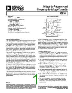
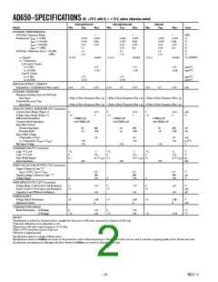
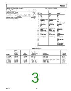
AD650
CIRCUIT OPERATION
UNIPOLAR CONFIGURATION
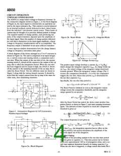
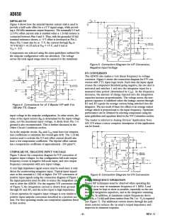
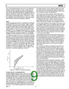
The AD650 is a charge balance voltage-to-frequency converter. In
the connection diagram shown in Figure 1, or the block diagram
of Figure 2a, the input signal is converted into an equivalent cur-
rent by the input resistance RIN. This current is exactly balanced
by an internal feedback current delivered in short, timed bursts
from the switched 1 mA internal current source. These bursts of
current may be thought of as precisely defined packets of charge.
The required number of charge packets, each producing one
pulse of the output transistor, depends upon the amplitude of
the input signal. Since the number of charge packets delivered
per unit time is dependent on the input signal amplitude, a linear
voltage-to-frequency transformation will be accomplished. The
frequency output is furnished via an open collector transistor.
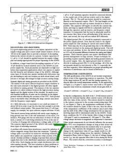
Figure 2b. Reset Mode
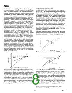
Figure 2c. Integrate Mode
A more rigorous analysis demonstrates how the charge balance
voltage-to-frequency conversion takes place.
A block diagram of the device arranged as a V-to-F converter is
shown in Figure 2a. The unit is comprised of an input integra-
tor, a current source and steering switch, a comparator and a
one-shot. When the output of the one-shot is low, the current
steering switch S1 diverts all the current to the output of the op
amp; this is called the Integration Period. When the one-shot
has been triggered and its output is high, the switch S1 diverts
all the current to the summing junction of the op amp; this is
called the Reset Period. The two different states are shown in
Figure 2 along with the various branch currents. It should be
noted that the output current from the op amp is the same for
either state, thus minimizing transients.
Figure 2d. Voltage Across CINT
The positive input voltage develops a current (IIN = VIN/RIN)
which charges the integrator capacitor CINT. As charge builds up
on CINT, the output voltage of the integrator ramps downward
towards ground. When the integrator output voltage (Pin 1)
crosses the comparator threshold (–0.6 volt) the comparator
triggers the one shot, whose time period, tOS is determined by
the one shot capacitor COS
.
Specifically, the one shot time period is:
tOS = COS × 6.8 ×10³ sec/F + 3.0 ×10⁻⁷ sec
(1)
The Reset Period is initiated as soon as the integrator output
voltage crosses the comparator threshold, and the integrator
ramps upward by an amount:
dV
tOS
∆V = tOS
•
=
1mA– I
(
)
(2)
N
dt CINT
After the Reset Period has ended, the device starts another Inte-
gration Period, as shown in Figure 2, and starts ramping downward
again. The amount of time required to reach the comparator
threshold is given as:
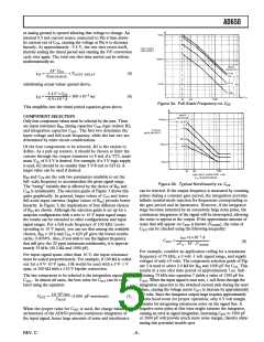
Figure 1. Connection Diagram for V/F Conversion,
Positive Input Voltage
t
OS/CINT(1mA – IIN )
1mA
IIN
∆
–1
V
(3)
TI =
=
= tOS
dV
dt
IN/CINT
The output frequency is now given as:
IIN
+ TI tOS ×1mA
V
IN/RIN
1
F Hz
•
A
fOUT
=
=
= 0.15
(4)
COS + 4.4 ×10⁻¹¹
F
tOS
Note that CINT, the integration capacitor has no effect on the
transfer relation, but merely determines the amplitude of the
sawtooth signal out of the integrator.
One Shot Timing
A key part of the preceding analysis is the one shot time period
that was given in equation (1). This time period can be broken
down into approximately 300 ns of propagation delay, and a sec-
ond time segment dependent linearly on timing capacitor COS
When the one shot is triggered, a voltage switch that holds Pin 6
.
Figure 2a. Block Diagram
–4–
REV. C

 ADI [ ADI ]