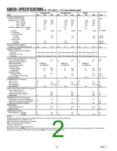
(@ +25؇C, with V = ؎15 V, unless otherwise noted)
AD650–SPECIFICATIONS
S
AD650J/AD650A
AD650K/AD650B
Typ
AD650S
Typ
Model
Min
Typ
Max
Min
Max
Min
Max
Units
DYNAMIC PERFORMANCE
Full-Scale Frequency Range
Nonlinearity1 fMAX = 10 kHz
Nonlinearity1 fMAX = 100 kHz
Nonlinearity1 fMAX = 500 kHz
Nonlinearity1 fMAX = 1 MHz
Full-Scale Calibration Error2, 100 kHz
Full-Scale Calibration Error2, 1 MHz
vs. Supply3
1
1
1
MHz
%
%
%
%
%
%
0.002
0.005
0.02
0.1
5
10
0.005
0.02
0.05
0.002
0.005
0.02
0.05
5
0.005
0.02
0.05
0.1
0.002
0.005
0.02
0.05
5
0.005
0.02
0.05
0.1
10
10
–0.015
+0.015
–0.015
+0.015
–0.015
+0.015
% of FSR/V
vs. Temperaturc
A, B, and S Grades
at 10 kHz
at 100 kHz
75
150
75
150
75
150
ppm/°C
ppm/°C
J and K Grades
at 10 kHz
at 100 kHz
75
150
75
150
ppm/°C
ppm/°C
BIPOLAR OFFSET CURRENT
Activated by 1.24 kΩ Between Pins 4 and 5
0.45
0.5
0.55
0.45
0.5
0.55
0.45
0.5
0.55
mA
DYNAMIC RESPONSE
Maximum Settling Time for Full Scale
Step Input
Overload Recovery Time
Step Input
1 Pulse of New Frequency Plus 1 µs 1 Pulse of New Frequency Plus 1 µs 1 Pulse of New Frequency Plus 1 µs
1 Pulse of New Frequency Plus 1 µs 1 Pulse of New Frequency Plus 1 µs 1 Pulse of New Frequency Plus 1 µs
ANALOLG INPUT AMPLIFIER (V/F Conversion)
Current Input Range (Figure 1)
Voltage Input Range (Figure 5)
Differential Impedance
0
–10
+0.6
0
0
–10
+0.6
0
0
–10
+0.6
0
mA
V
2 MΩʈ10 pF
2 MΩʈ10 pF
2 MΩʈ10 pF
Common-Mode Impedance
Input Bias Current
1000 MΩʈ10 pF
1000 MΩʈ10 pF
1000 MΩʈ10 pF
Noninverting Input
Inverting Input
40
8
100
؎20
40
8
100
؎20
40
8
100
؎20
nA
nA
Input Offset Voltage
(Trimmable to Zero)
؎4
؎4
؎4
mV
vs. Temperature (TMIN to TMAX
Safe Input Voltage
)
30
VS
30
30
µ V/°C
C
VS
VS
COMPARATOR (F/V Conversion)
Logic “0” Level
–VS
0
0.1
–1
+VS
(0.3 × tOS
–VS
0
0.1
–1
+VS
(0.3 × tOS
–VS
0
0.1
+1
+VS
(0.3 × tOS
V
V
µs
kΩ
Logic “1” Level
Pulse Width Range4
Input Impedance
)
)
)
250
250
250
OPEN COLLECTOR OUTPUT (V/F Conversion)
Output Voltage in Logic “0”
ISINK ≤ 8 mA, TMIN to TMAX
0.4
100
+36
0.4
100
+36
0.4
100
+36
V
nA
V
Output Leakage Current in Logic “1”
Voltage Range5
0
0
0
AMPLIFIER OUTPUT (F/V Conversion)
Voltage Range (1500 Ω min Load Resistance)
Source Current (750 Ω max Load Resistance)
Capacitive Load (Without Oscillation)
0
10
+10
100
0
10
+10
100
0
10
+10
100
V
mA
pF
POWER SUPPLY
Voltage, Rated Performance
Quiescent Current
9
؎18
8
9
؎18
8
9
؎18
8
V
mA
TEMPERATURE RANGE
Rated Performance – N Package
0
–25
+70
+85
0
–25
+70
+85
°C
°C
Rated Performance –
D Package
–55
+125
NOTES
1Nonlinearity is defined as deviation from a straight line from zero to full scale, expressed as a fraction of full scale.
2Full-scale calibration error adjustable to zero.
3Measured at full-scale output frequency of 100 kHz.
4Refer to F/V conversion section of the text.
5Referred to digital ground.
Specifications subject to change without notice.
Specifications shown in boldface are tested on all production units at final electrical test. Results from those test are used to calculate outgoing quality levels. All min and max
specifications are guaranteed, although only those shown in boldface are tested on all production units.
–2–
REV. C

 ADI [ ADI ]