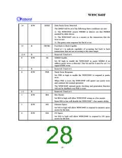
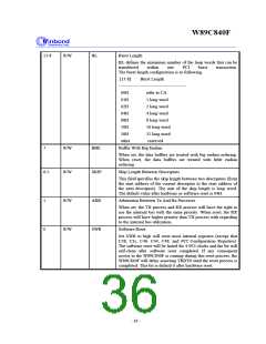
W89C840F
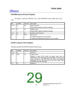
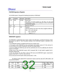
F40/FSR Signature Register
The F40/FSR register is designed for identifying the hardware of W89C840F.
Bit
Attribute
R/W
Bit name
DVAR
Description
Driver Area
31:16
This field is for driver special use. The driver can write some
specific pattern to these bits for bundling the software and hardware
of W89C840F together.
15:8
7:0
R
R
---
Reserved. Fixed at 0.
SIG
Signature.
After the hardware reset, these 8 bits value is toggled as following
SIG = 12H at (2N-1)th read
9AH at 2Nth read
where N= 1, 2, ....
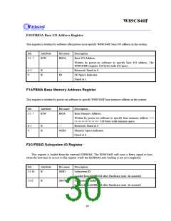
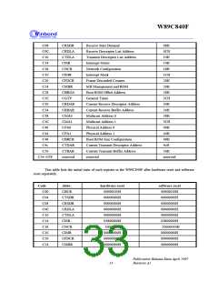
W89C840F registers
The W89C840F is implemented many registers, listed in the table below, to perform the function control
and monitor the status of MAC.The general attributes of the W89C840F register is described as the
following:
1) The W89C840F registers are mapped into the host I/O or memory space.
2) The registers of the W89C840F are long word-aligned. Each register consists of 32 bits and may be
accessed using any byte enable combinations with long word-aligned address.
3) The byte enabling and addressing must meet the specification for I/O access addressing rule when the
register is in I/O space.
4) Burst access to the W89C840F register will be terminated after 1st data transfer completed with a
Disconnect without Data.
5) S/W reset will have the same effect as done by H/W reset on the W89C840F register, except for the
registers or bits C00<0>, C38, C3c, C40, C44, C48.
6) Any read on the reserved register will be returned with 0‘ s value.
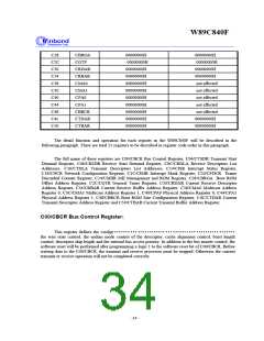
The following table outlined all the control/status registers inside this chip and its offset address, and
summarized its function.
Code
Abbr.
Meaning
Base offset from
FBIOA, FBMA
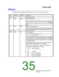
C00
C04
CBCR
Bus Control
00H
04H
CTSDR
Transmit Start Demand
- 32 -

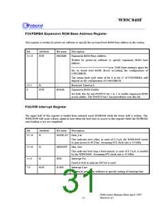
 ETC [ ETC ]