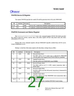
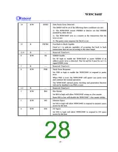
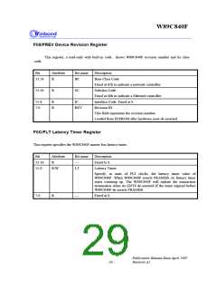
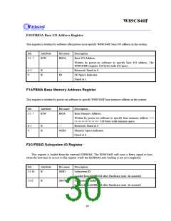
W89C840F
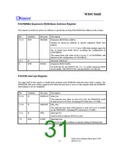
F30/FERBA Expansion ROM Base Address Register
This register is written by power-on software to specify the on-board boot ROM base address in the system.
Bit
Attribute
R/W
Bit name
EROMB
Description
31:13
Expansion ROM Base Address.
Written by power-on software to specify expansion ROM base
address.
The W89C840F wi l l r equest up to 256K bytes memory space for
the on board boot ROM device according the configuration of
C48/CBRCR.
The return back read value of bit 0 to bit 17 of F30/FERBA will
depend on the configuration of C48/CBRCR.
12:1
0
R
---
Reserved. Fixed at 0.
R/W
ROME
Expansion ROM Enable.
Set both this bit and F04/FCS bit 1 to 1 to enable expansion ROM
access ability. The F04/FCS bit 1 has precedence over this bit.
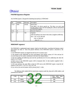
F3C/FIR Interrupt Register
The upper half of this register is loaded from external serial EEPROM while the lower half is written. The
W89C840F will issue a Retry signal to host when the host tries to access to this register while the EEPROM
auto-loading is not yet completed.
Bit
Attribute
R
Bit name
MAXLAT Max_Lat.
This indicates how often, in units of 0.25mS, the W89C840F needs
to gain access to PCI bus. Assuming PCI clock rate is 33 MHz.
MINGNT Min_Gnt.
Description
31:24
23:16
R
This indicates how long a burst period, in units of 0.25mS, is needed
by the W89C840F. Assuming PCI clock rate is 33 MHz.
15:8
7:0
R
IPIN
Interrupt Pin.
Fixed at 01H to indicate INTA# is used.
Interrupt Line.
R/W
ILINE
Written by power-on software to specify routing of interrupt line.
Publication Release Date:April 1997
- 31 -
Revision A1

 ETC [ ETC ]