W89C840F
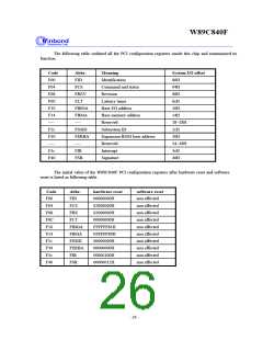
The following table outlined all the PCI configuration registers inside this chip and summarized its
function.
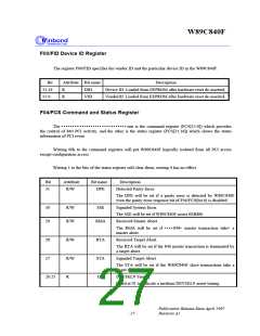
Code
F00
F04
F08
F0C
F10
F14
----
Abbr.
FID
Meaning
System I/O offset
Identification
Command and status
Revision
00H
FCS
04H
FREV
FLT
08H
Latency timer
Base I/O address
Base memory address
Reserved
0cH
FBIOA
FBMA
----
10H
14H
18~28H
2cH
F2c
F30
----
FSSID
FERBA
----
Subsystem ID
Expansion ROM base address
Reserved
30H
34~38H
3cH
F3c
F40
FIR
Interrupt
FSR
Signature
40H
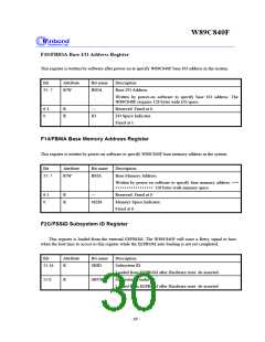
The initial value of the W89C840F PCI configuration registers after hardware reset and software
reset is listed as following table.
Code
F00
F04
F08
F0C
F10
F14
F2c
F30
F3c
F40
Abbr.
FID
hardware reset
00000000H
02800000H
02000000H
00000000H
FFFFFF81H
FFFFFF80H
00000000H
00000000H
00000100H
00000012H
software reset
non affected
non affected
non affected
non affected
non affected
non affected
non affected
non affected
non affected
non affected
FCS
FRE
FLT
FBIOA
FBMA
FSSID
FERBA
FIR
FSR
- 26 -

 ETC [ ETC ]