W89C840F
latched by the bit 3 of CMIIR, and be read by W89C840F. The application program can program bits
0, 1 and 2 of CMIIR to generate the chip select signal, clock and read command, based on the AC
timing spec. of the EEPROM device, to EEPROM, and running over the pins EECS, BtAdata1/EECK,
and BtAdata2/EEDI respectively. For reading the output data from EEPROM, the application program
should make the necessary level transition as a clock on BtAdata1/EECK. One falling edge will trigger
the EEPROM device to drive the next bit of output data relative to the input command.
The EEPROM can be programmed through the general I/O port of the W89C840F. The
application program can write data into the EEPROM through programming the bits 0, 1 and 2 of the
register CMIIR. In the write cycle of the EEPROM device, the data on BtAdata3/EEDO is
meaningless.
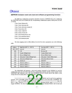
BOOT ROM system read and software programming function
The W89C840F can address up to 256 Kbytes memory space for the on-board boot ROM
device. The on-board boot ROM device will be mapped into the host memory by the system BIOS
(Basic Input/Output System). After power-on reset, The BIOS will write a set of value with all 1 to the
F30/FERBA configuration register and then read the value back. The W89C840F will return the all 1
value, except some bits with 0, depending on the configuration of C48/CBRCR. The relationship
between the return value from the register F30/FERBA and the setting to the register C48/CBRCR is
described as the following table.
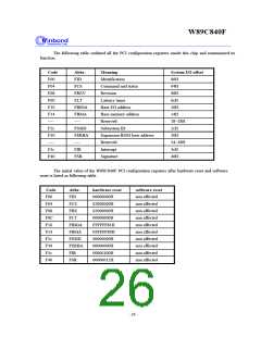
ROM size
No boot ROM
No boot ROM
C48/CBRCR configuration
00000000H
F30/FERBA return value
00000000H
00000001H
00000000H
8
Kbytes ROM
00000002H
FFFFE001H
FFFFC001H
FFFF8001H
16 Kbytes ROM
32 Kbytes ROM
64 Kbytes ROM
128 Kbytes ROM
256 Kbytes ROM
00000003H
00000004H
00000005H
FFFF0001H
00000006H
FFFE0001H
00000007H
FFFC0001H
According to the return value from the register F30/FERBA, The system BIOS can determine
how large the memory space is required and then writes the memory space base address back to the
register F30/FERBA. In the cases of no boot ROM, the system BIOS will write back all 0 back into
F30/FERBA.
The address decoder of W89C840F for accessing the on-board ROM memor y wi l l be enabl ed
i f bot h bi t 0 of F30/ FERBA and bit 1 of F04/FCS are set to high at the same time. The on-board
boot ROM data will be fetched by W89C840F and loaded into the host memory. On the other hand, the
address decoder will be disabled if the bit 0 of F30/FERBA is reset to 0. Under this case, W89C840F will
ignore the C48/CBRCR, no matter what content it has.
Publication Release Date:April 1997
- 23 -
Revision A1

 ETC [ ETC ]