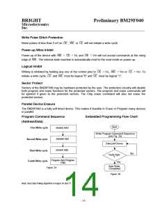
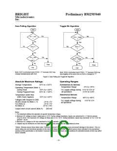
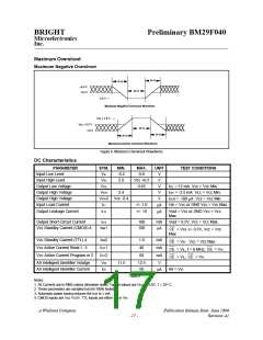
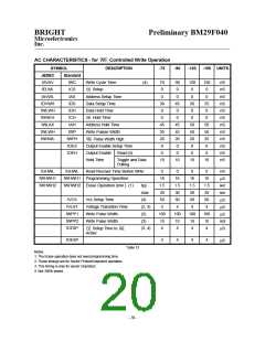
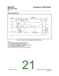
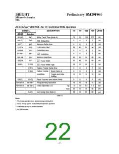
BRIGHT
Microelectronics
Inc.
Preliminary BM29F040
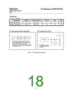
Capacitance:
TA = 25° C, f = 1 MHZ (2)
PARAMETER
Input Capacitance
Output Capacitance
SYMBOL
Cin
CONDITIONTION
Vin = 0V
TYPICAL
MAX.
8
UNIT
pF
6
Cout
Vout = 0V
10
12
pF
AC Testing Input/Output Waveform
AC Testing Load Circuit
2.7K
R
L
2.4
2.0
0.8
2.0
0.8
Test
Points
Input
0.45
Output
Device Under
Test
AC test inputs are driven at Voh ( 2.4V VTTL) for a
logic "1" and Vol ( 0.4V VTTL) for a logic "0". Input
timing measurement begins at Vih ( 2.0V VTTL) for an
input "1" and Vil ( 0.8V VTTL) fir an input "0".
Output timing measurement ends at 2.0V for an output
"1" and 0.8V for an output "0". Input Rise and fall times
(10% to 90%) <10 nS.
R
C
L
L
6.2K
C
= 100 pF
L
L
C
includes Jig Capacitance
The diodes are 1N3064 or
wequivalent.
Figure 7. A.C.Testing Load and Waveforms
- 18 -

 WINBOND [ WINBOND ]