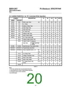
BRIGHT
Microelectronics
Inc.
Preliminary BM29F040
Data Polling Algorithm
Toggle Bit Algorithm
Start
Start
Yes
No
7
DQ = Data
6
DQ = Toggle
?
?
No
Yes
No
No
DQ 5=1
DQ5=1
?
?
Yes
Yes
Note 2
DQ 6 = Toggle
Yes
DQ 7= Data
?
Note 1
No
?
No
Yes
Pass
Pass
Fail
Fail
Note: DQ7 is rechecked even if DQ5 = "1" because DQ7 may
change simultaneously with DQ5.
Note: DQ6 is rechecked even if DQ5 = "1" because DQ6 may
stop toggling at the same time as DQ5 is changed to "1".
Figure 5. Data Polling and Toggle Bit Algorithm
Absolute Maximum Ratings:
Operating Ranges:
Commercial (C) Devices
Storage Temperature
-65°C to +125°C
Temperature Range
0°C to +70°C
Operating Temperature (Note 1)
Vcc supply voltage during 4.5V to 5.5V or
During Read
-55°C to +125°C
all operations
4.75V to 5.25V
During Program/Erase
-55°C to +125°C
Industrial (I) Devices
Temperature Range
Temperature under Bias
(With Power Applied)
-55°C to +125°C
-40°C to +85°C
Voltages with Respect to GND.
All pins except A9 (Note 2, 3)
Vcc (Note 2)
Vcc supply voltage during
all operations
4.5V to 5.5V
-2V to +7V
-2V to +7V
-2V to +14V
A9 (Note 3)
Output short circuit current (Note 4)
200 mA
Notes :
1. The datasheet defines the operation at specific temperature ranges.
2. Minimum DC voltage on input / output pins is -0.5V. During voltage transitions, inputs can undershoot to -2 Volts for periods
of up to 20 nS. The maximum DC voltage on these pins is Vcc +0.5V. During transitions, inputs may overshoot to Vcc +2.0V for
periods < 20 nS.
3. Maximum DC voltage on A9 may overshoot to 14.0V for periods < 20 nS.
4. Outputs may be shorted for no more than one second. Only one/output can be shorted at a time.
*Notice: Stresses above those listed under "Absolute Maximum Ratingsz" may cause permanent damage to the device. This is a
stress rating only and functional operation of the device at these or any other conditions above those indicated in the operational
sections of this specification is not implied. Exposure to absolute maximum rating conditions for extended periods of time may affect
device reliability.
- 16 -

 WINBOND [ WINBOND ]