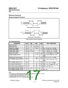
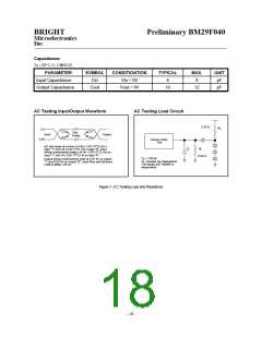
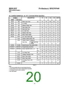
BRIGHT
Microelectronics
Inc.
Preliminary BM29F040
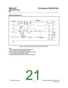
Switching Waveforms
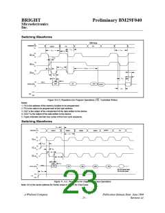
Data Polling
Vih
Addresses (A)
PA
PA
5555H
tWC
Vil
AH
t
RC
t
tAS
Vih
Vil
CE (E)
tGHWL
Vih
Vil
OE (G)
tWPH
CS
t
WHWH1
t
Vih
Vil
WE (W)
DF
t
tWP
tOH
DS
t
t OE
Vih
Vil
DH
t
HIGH Z
DATA (D/Q)
DQ7
PD
A0H
DOUT
CE
t
5.0 V
VCC
GND
Figure 9. A.C.Waveforms for Program Operations ( WE Controlled Writes)
Notes:
1. PA is the address of the memory location to be programmed.
2. PD is the data to be programmed at the byte address.
3. DQ7 is the output of the complement of the data written tot he device.
4. DOUT is the output of the data written to the device.
5. Figure indicates the last two bus cycles of four bus cycle sequence.
A Winbond Company
- 21 -
Publication Release Date: June 1999
Revision A1

 WINBOND [ WINBOND ]