BRIGHT
Microelectronics
Inc.
Preliminary BM29F040
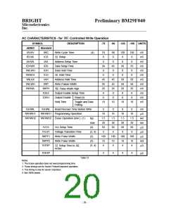
AC Characteristics - Read Only Operations (1)
SYMBOL (4)
DESCRIPTION
-75 -90
-120
-150
UNITS
JEDEC
Standard
tRC
tAVAV
tAVQV
tELQV
Read Cycle Time
Address to Output Delay
70
70
70
90
90
90
120
120
120
150
150
150
nS
nS
nS
tACC
tCE
(2)
(3)
low to Output Delay
low to Output Delay
low to Output LOW Z
high to Output HIGH Z
low to Output LOW Z
high to Output HIGH Z
CE
OE
CE
CE
OE
OE
tGLQV
tELQX
tEHQZ
tGLQX
tGHQZ
tAXQX
tOE
tLZ
30
0
35
0
50
0
55
0
nS
nS
nS
nS
nS
nS
tHZ
20
0
20
0
30
0
35
0
tOLZ
tDF
(3)
(1)
20
0
20
0
30
0
35
0
tOH
Output Hold from Address,
or
, whichever is first
CE
OE
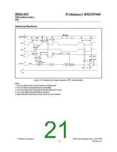
Table 11
Notes:
1. See A.C. Input/Output Reference Waveforms for timing measurements.
2. may be delayed up to tCE-tOE after the falling edge of without impact on tCE.
OE
3. Sampled, not 100% tested.
4. See A.C. Input/Output Reference Waveforms and A.C. Testing Load Circuits for testing characteristics.
CE
Vcc Power-
up
Device &
Outputs
Enabled
Vcc Power-
Standby
Data Valid
Standby
Address Select.
down
t AVAV
Vih
Addresses
Address Valid
Vil
Vih
Vil
CE (E)
OE (G)
WE (W)
t EHQZ
Vih
Vil
t GHQZ
t
GLQV
Vih
ELQV
t
Vil
AVQV
t
AXQX
t
Vih
t
GLQX
High Z
High Z
DATA (D/Q)
Vil
Valid Output
ELQX
t
5.0 V
VCC
GND
Figure 8. A.C.Waveforms for Read Operations
A Winbond Company
Publication Release Date: June 1999
Revision A1
- 19 -

 WINBOND [ WINBOND ]