BRIGHT
Microelectronics
Inc.
Preliminary BM29F040
Write Pulse Glitch Protection
Noise pulses of less than 5 nS on OE , WE or CE will not initiate a write cycle.
Power-up Wtire Inhibit
Power-up of the device with WE = CE = VIL and OE = VIH will not accept commands at the rising
edge of WE . The internal state machine is automatically reset to the read mode on power-up.
Logical Inhibit
Writing is inhibited by holding any one of the control pins to OE = VIL, WE = VIH or CE = VIH. To
initiate a write cycle, CE and WE must be logical "0" and OE must be logical "1".
Sector Protect
Sectors of the BM29F040 may be hardware protected by the user. The protection circuitry will disable
both program and erase functions for the protected sectors. The program and erase commands will
be ignored if given to the protected sectors. The Chip erase command will also not erase the
protected sectors.
Parallel Device Erasure
The BM29F040 is a fully self timed device. This makes it feasible to Erase or Program many devices
in parallel.
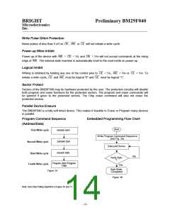
Program Command Sequence
(Address/Data)
Embedded Programming Flow Chart
Start
First Write cycle
5555H/ AAH
2AAAH/ 55H
5555H/ A0H
Write Program Command Sequence
(see Fig. 3a)
Second Write cycle
Data poll Device
Third Write cycle
Fourth Write cycle
No
Verify Byte
?
Program Add./Program
Data
Yes
Byte Write
Completed
Figure: 3A
Figure: 3B
Note: See Data Polling Algorithm in Figure 10 and 11.
- 14 -

 WINBOND [ WINBOND ]