OX9162
OXFORD SEMICONDUCTOR LTD.
6.3 Register Description
The parallel port registers are described below. (NB it is assumed that the upper block is placed 400h above the lower block).
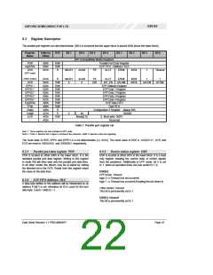
Register
Name
Address R/W
Offset
Bit 7
Bit 6
Bit 5
Bit 4
Bit 3
Bit 2
Bit 1
Bit 0
SPP (Compatibility Mode) Registers
PDR
ecpAFifo
DSR
(EPP mode)
000h
000h
001h
R/W
R/W
R
Parallel Port Data Register
ECP FIFO : Address / RLE
nBUSY
ACK#
PE
SLCT
ERR#
INT#
1
Timeout
(Other modes)
001h
002h
003h
004h
005h
006h
007h
400h
400h
400h
401h
402h
403h
R
nBUSY
0
ACK#
0
PE
DIR
SLCT
ERR#
INT#
INIT#
1
1
DCR
EPPA 1
EPPD1 1
EPPD2 1
EPPD3 1
EPPD4 1
EcpDFifo
TFifo
R/W
R/W
R/W
R/W
R/W
R/W
R/W
R/W
R
INT_EN nSLIN#
EPP Address Register
EPP Data 1 Register
EPP Data 2 Register
EPP Data 3 Register
EPP Data 4 Register
ECP Data FIFO
nAFD#
nSTB#
Test FIFO
CnfgA
CnfgB
ECR
Configuration A Register – always 90h
‘000000’
R
R/W
-
0
int
Mode[2:0]
Must write ‘00001’
Reserved
-
Table 7: Parallel port register set
Note 1 : These registers are only available in EPP mode.
Note 2 : Prefix ‘n’ denotes that a signal is inverted at the connector. Suffix ‘#’ denotes active-low signalling
The reset state of PDR, EPPA and EPPD1-4 is not determinable (i.e. 0xXX). The reset value of DSR is ‘XXXXX111’. DCR and
ECR are reset to ‘0000XXXX’ and ‘00000001’ respectively.
6.3.1 Parallel port data register ‘PDR’
6.3.3 Device status register ‘DSR’
PDR is located at offset 000h in the lower block. It is the
standard parallel port data register. Writing to this register
in mode 000 will drive data onto the parallel port data lines.
In all other modes the drivers may be tri-stated by setting
the direction bit in the DCR. Reads from this register return
the value on the data lines.
DSR is located at offset 001h in the lower block. It is a read
only register showing the current state of control signals
from the peripheral. Additionally in EPP mode, bit 0 is set
to ‘1’ when an operation times out (see section 6.1.3)
DSR[0]:
EPP mode: Timeout
logic 0 Þ Timeout has not occurred.
logic 1 Þ Timeout has occurred (Reading this bit clears it).
6.3.2 ECP FIFO Address / RLE
A data byte written to this address will be interpreted as an
address if bit(7) is set, otherwise an RLE count for the next
data byte. Count = bit(6:0) + 1.
Other modes: Unused
This bit is permanently set to 1.
DSR[1]: Unused
This bit is permanently set to 1.
Data Sheet Revision 1.1 PRELIMINARY
Page 22

 OXFORD [ OXFORD SEMICONDUCTOR ]