OX9162
OXFORD SEMICONDUCTOR LTD.
means that I/O space can be allocated efficiently by the
system, whatever the application.
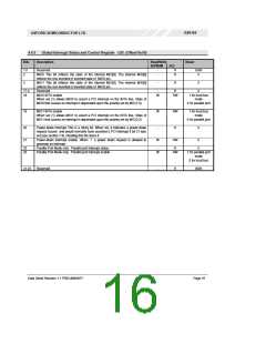
5.3 Configuration & Programming
The configuration registers for the local bus controller are
described in sections 4.4.3 & 4.4.4. The values of these
registers after reset allow the host system to identify the
function and configure its base address registers.
Alternatively many of the default values can be re-
programmed during device initialisation through use of the
optional serial EEPROM (see section 7).
The memory space block is always 4K bytes, and always
divided into two chip-select regions of 2K byte each (only
the bottom 1K of each is accessible).
A
soft reset facility is provided so software can
independently reset the peripherals on the local bus. The
local bus reset signals, LBRST and LBRST#, are always
active during
configuration register bit LT2[29] is set to 1.
a PCI bus reset and also when the
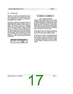
There is one I/O block space defined for each chip select.
The I/O space blocks can be varied in size from 4 bytes to
256 bytes (8 bytes is the default) by setting LT2[22:20]
(BAR 0) and LT2[26:24] (BAR 1). Varying the block size
The clock enable bit, when set, enables a copy of the PCI
bus clock output on the local bus pin LBCLK.
Data Sheet Revision 1.1 PRELIMINARY
Page 20

 OXFORD [ OXFORD SEMICONDUCTOR ]