FEDL87V2107-01
OKI Semiconductor
ML87V2107
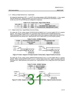
1.2.6 Setting Output Detection field Inversion
By setting the I2C-bus setting register OFINV(SUB:61h-bit[3]), internal field detection can be inverted.
Table F1-2-6 OFINV Setting
Input field
OFINV
Field A
Field B
0
1
0
1
1
0
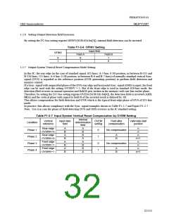
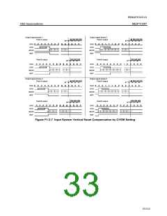
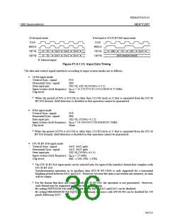
1.2.7 Output System Vertical Reset Compensation Mode Setting
In this IC, the rear edge (in the case of standard signal, 625 lines; A-3 line, 0.5H position, in between B-315 and
B-316 lines, 525 lines; A-6 line, 0.5H position, in between B-6 and B-7 lines) of normally standard vertical Sync.
signal (OVS) is regarded as the reference position (OVR generating position) to perform field detection and
memory control.
If a Sync. signal with unspecified phase of the OVS rear edge and horizontal Sync. signal (OHS) is input, the front
edge can be used with the setting OVSINV = 1. But if the front edge is used in standard 626-line mode, the
detection filed reverses in normal operation and field B gets written in the memory with one line earlier phase.
Therefore, by setting the I2C-bus setting register OVEM (SUB:61h-bit[4]), the detection field is inverted (ARB,
BRA) and the vertical phase with regard to field B of the inverted result is delayed by 1H.
This allows compensation for field detection and OVR which is the typical front edge phase of OVS of 625-line
mode.
In practice, this allows compliance with the Sync. signal examples shown in Table F1-2-7 and Figure F1-2-7
Note: Use it in case the phase of field-detecting OVS and OHS reverses in the IC standard setting.
Table F1-2-7 Input System Vertical Reset Compensation by OVEM Setting
Internal
determination
field
Vertical
reference
Input data
field
OVEM
setting
Field after
compensation
Valid data start
position
Condition
Rear edge
OVSINV=0
Rear edge
OVSINV=0
Front edge
OVSINV=1
Front edge
OVSINV=1
A
B
A
B
A
B
A
B
A
B
B
A
A
B
B
A
n
n
Phase 1
Phase 2
Phase 3
Phase 4
0
1
0
1
No compensation
A
B
n
n+1
n
No compensation
n
A
B
n
n+1
32/152

 OKI [ OKI ELECTRONIC COMPONETS ]