FEDL87V2107-01
OKI Semiconductor
ML87V2107
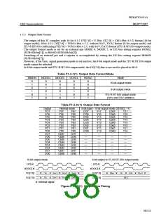
1.2.8 Output Control
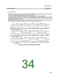
Under fOCLK = fIICLK, fOVS = fIVS, and fOHS = fIHS, this IC outputs frame memory data from the memory control signals
that are generated from standard output Sync. signal OVS and OHS.
In this case, the field of the memory data and the field of the output OVS and OHS must match.
For the phase in which the field of the memory data and the output Sync. signal field match, the internal output
read enable (ORE) generated phase that occurs in OVS of the field delays by 1 line to 2 fields compared to internal
write enable (IWE) that occurs in IVS.
When the phases of IVS and OVS are close and ICLK and OCLK are not locked, the phases must be adjusted to
prevent overtaking by the memory address by IVS and the memory address by OVS.
Afield:n
Bfield;n
Afield:n+1
Bfield:n+1
IVS
#IF
Memory
data
Bn-1
An
Bn
An+1
Bn+1
[1-line delay between IVS and OVS]
Afield:n
OVS
Bfield;n
Afield:n+1
Bfield:n+1
#OF
YO
CO
An+1
Bn+1
An+2
An
Bn
[1-field delay between IVS and OVS]
Bfield:n-1
OVS
Afield:n
Bfield;n
Afield:n+1
#OF
YO
Bn-1
CO
An
Bn
An+1
Bn+1
#: Internal signal
Figure F1-2-8(1) Normal Mode Output Timing
34/152

 OKI [ OKI ELECTRONIC COMPONETS ]