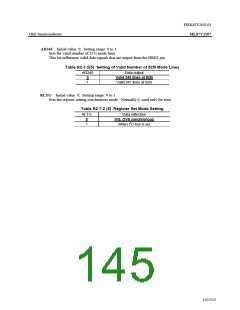
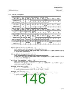
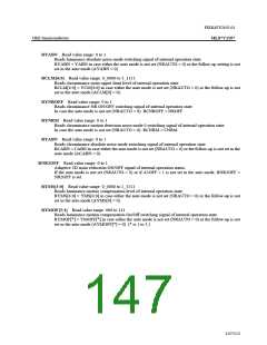
FEDL87V2107-01
OKI Semiconductor
ML87V2107
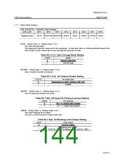
2.7.2 Other Mode Settings
SUB_ADDRESS = 72h(W/R): Other settings
DATA_BIT
BIT7
BIT6
BIT5
BIT4
BIT3
BIT2
BIT1
BIT0
(Reserved) (Reserved)
Register name
RLTG
AR241
ABLK
OEINV OUTDS PASS
PASS Initial value: 0; Setting range: 0 to 1
Sets data through mode.
The input pin is directly connected to the output pin. At this time, there is a delay generated equal to the
time it takes for the output data to pass through the internal circuitry.
Table R2-7-2 (1) Data Through Mode Setting
PASS
Mode
0
Normal operation
Data through
1
OUTDS Initial value: 0; Setting range: 0 to 1
Sets to disable forcibly all outputs.
Table R2-7-2 (2) All Outputs Disable Setting
OUTDS
All output pins
Dependent on other settings (OE, INT)
Disable
0
1
OEINV Initial value: 0; Setting range: 0 to 1
Sets OE input pin polarity inversion.
Table R2-7-2(3) OE Input Pin Polarity Inversion Setting
OEINV
OE input pin
0
OE = 0: Output data disable
OE = 1: Output data disable
1
ABLK Initial value: 0; Setting range: 0 to 1
Sets total blanking level output.
This bit is valid in memory output mode only.
Table R2-7-2(4) All Blanking Level Output Setting
ABLK
Data output
0
Normal output
Blanking level output
(YO[7:0] = BLS[1:0] setting value, CO[7:0] = 80h)
1
144/152

 OKI [ OKI ELECTRONIC COMPONETS ]