FEDL87V2107-01
OKI Semiconductor
ML87V2107
2.6 Sync. Signal Generation Settings
2.6.1 Sync. Signal Generation Mode Settings
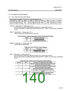
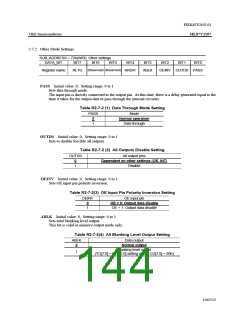
SUB_ADDRESS=68h(W/R): Sets the Sync. signal generation mode.
DATA_BIT
BIT7
BIT6
BIT5
BIT4
BIT3
BIT2
BIT1
BIT0
Register name (Reserved)
IINT
(Reserved) (Reserved) HSSEL
SFINV (Reserved) IASYNC
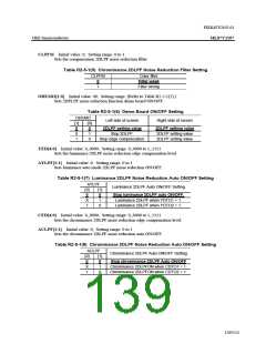
IASYNC Initial value: 0; Setting range: 0 to 1
Sets the generation mode of the internal generation Sync. signals OHS and OVS.
However, this register is enabled only when external pin INT = 0, DNR = 0 (external pin), and IDNR=0
are set.
SFINV Initial value: 0; Setting range: 0 to 1
Sets the field of internal generation OVS and OHS.
Table R2-6-1(1) Internal Generation OVS and OHS Field Setting
SFINV
OVS and OHS phase
In phase with write
0
1
In inverted phase with write
HSSEL Initial value: 0; Setting range: 0 to 1
Sets the OHS pin output signal.
Table R2-6-1(2) OHS Pin Output Setting
HSSEL
OHS phase
0
Horizontal Sync. signal
Composite Sync. signal
1
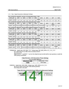
IINT Initial value: 0; Setting range: 0 to 1
Sets the generation mode of the internal generation Sync. signals OHS and OVS.
However, this register is enabled only when external pin INT = 0, DNR = 0 (external pin), and IDNR=0
are set.
Table F2-6-1(3) OHS and OVS Generation Mode Setting
IASYNC
IINT
OHS and OVS generation mode setting
Internal synchronous generation stop mode (external
synchronous frame buffer output)
0
0
IVS reset synchronous generation mode (Input vertical
synchronous frame buffer output)
0
1
1
1
0
1
TRG reset synchronous generation mode
(Frame-trigger- vertical synchronous frame buffer
output)
OCLK-dividing synchronous generation mode
(Asynchronous frame buffer output)
140/152

 OKI [ OKI ELECTRONIC COMPONETS ]