FEDL87V2107-01
OKI Semiconductor
ML87V2107
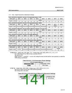
2.6.2 Sync. Signal Generation Adjustment Settings
SUB_ADDRESS=69h(W/R): Sets the OVS generation phase. (LSB)
DATA_BIT
BIT7
BIT6
BIT5
BIT4
BIT3
3
BIT2
2
BIT1
BIT0
0
SVDL
Register name
7
6
5
4
1
SUB_ADDRESS=6Ah(W/R): Sets the OVS generation phase. (MSB)
DATA_BIT BIT7 BIT6 BIT5 BIT4
BIT3
BIT2
10
BIT1
SVDL
9
BIT0
8
Register name (Reserved) (Reserved) (Reserved) (Reserved) (Reserved)
SUB_ADDRESS=6Bh(W/R): Sets the phase difference between OVS and OHS.
DATA_BIT
BIT7
7
BIT6
6
BIT5
5
BIT4
4
BIT3
3
BIT2
2
BIT1
1
BIT0
0
SVD
Register name
SUB_ADDRESS=6Ch(W/R): Sets the OHS width adjustment.
DATA_BIT
BIT7
BIT6
BIT5
BIT4
BIT3
3
BIT2
2
BIT1
1
BIT0
0
SHW
Register name
7
6
5
4
SUB_ADDRESS=6Dh(W/R): Sets the synchronous delay adjustment.
DATA_BIT
BIT7
BIT6
BIT5
BIT4
BIT3
3
BIT2
2
BIT1
1
BIT0
0
SYDL
Register name
7
6
5
4
SUB_ADDRESS=6Eh(W/R): Sets horizontal Sync. signal generation.
DATA_BIT BIT7 BIT6 BIT5 BIT4
BIT3
BIT2
BIT1
1
BIT0
0
VSYM
Register name DSYNC (Reserved) (Reserved) (Reserved) (Reserved) (Reserved)
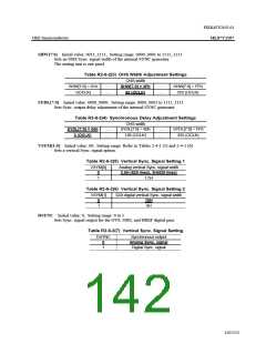
SVDL[10:0] Initial value: 000_0000_1111; Setting range: 000_0000_0000 to 111_1111_1111
Set a delay from IVS or TRG to the occurrence of OVS.
The unit is 0.5H.
When ASYNC = 1 and INT = 1 are set, the setting becomes invalid and the same operation as under the
000h setting is performed.
Table R2-6-2(1) OVS Generation Phase Settings
IVS-OVS phase difference
SVDL[10:0] = 000h
0 lines
SVDL[10:0] = 7FFh
1023.5 lines
……
……
SVD[7:0] Initial value: 0000_0000; Setting range: 0000_0000 to 1111_1111
Set an OVS delay for the OHS of the internal generator.
The setting unit is one pixel.
Table R2-6-2(2) OVS-OHS Phase Difference Adjustment Settings
OVS-OHS phase difference
SVD[7:0] = 00h
0 (OCLK)
SVD[7:0] = 80h
128 (OCLK)
SVD[7:0] = FFh
255 (OCLK)
……
……
……
……
141/152

 OKI [ OKI ELECTRONIC COMPONETS ]