VS1005g Datasheet
10 VS1005 PERIPHERALS AND REGISTERS
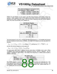
PLL value examples for most typical xtals
xtal frequency FMPLL register
12.0MHz 54402918 = 0x033E 1F66
12.288MHz 53127850 = 0x032A AAAA
13.0MHz 50218079 = 0x02FE 445F
FMCCF_HI and FMCCF_LO are used to set FM tuning frequency (FM Carrier Center Fre-
quency). These registers hold a 27-bit signed value which controls the frequency inside the
selected VCO center frequency range. This VCO center frequency is set with divider registers
ANA_CF3_DIV[1:0] and ANA_CF3_FMDIV[1:0].
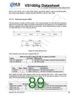
VCO Divider Register
ANA_CF3_DIV[1:0] VCO Divider
“00” 36
“01” = “10” 30
“11” 25
FM divider
ANA_CF3_FMDIV[1:0] FM divider
“00” 16
“10” 20
“11” = “01” 24
The VCO frequency is 24, 20 or 16 times the FM tuning frequency, i.e. for 95.0MHz FM channel
the VCO frequency must be set to 1.900GHz. The target VCO frequency can be calculated from
equation :
FMCCFreg
221
Fvco = (4 × V COdiv + CCF) × Fxtal where CCF is defined as CCF =
and the FM channel frequency can be given as:
+ 16
FFM = ((4 × V COdiv + CCF) × Fxtal)/FMdiv
For high speed USB FMCCF registers must be reset when 12.000MHz xtal is used. When
12.288MHz xtal is used the registers are initialized to 0xFF87, 0xFFFF (-7864321). FM_CF
register is initialized to value 0x0041. This makes VCO frequency of 1.92GHz which results to
480MHz USB clock.
FM_PHSCL Bits
Name
Bits Description
FM_PHSCL_I[7:0]
FM_PHSCL_Q[7:0]
15:8 I scaling factor
7:0 Q scaling factor
FM_PHSCL register is used to compensate I and Q signal’s phase and amplitude error. This
error depends from several factors and values should be calculated for each FM band. The
compensation logic is enabled when FM_CF_PHCOMP register is set. Typical values are 111
for I-scaling and 137 for Q-scaling.
Version: 0.2, 2012-03-16
88

 ETC [ ETC ]