VS1005g Datasheet
10 VS1005 PERIPHERALS AND REGISTERS
10.19 Timer Peripheral
Vs1005 has three 32-bit timers that can be initialized and enabled independently of each other.
If enabled, a timer initializes to its user initialized start value, and starts decrementing every
clock cycle. When the value goes past zero, an interrupt request is generated, and the timer
initializes to the value in its start value register, and continues downcounting. A timer stays in
that loop as long as it is enabled. Each timer has its own interrupt request.
A timer has a 32-bit timer register for down counting and a 32-bit TIMER1_LH register for
holding the timer start value written by the processor. Timers have also a 3-bit TIMER_ENA
register. Each timer is enabled (1) or disabled (0) by a corresponding bit of the enable register.
10.19.1 Timer Peripheral Registers
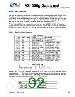
Timer Registers
Reg Type Reset Abbrev
Description
0xFE80
0xFE81
r/w
r/w
0
0
TIMERx_CFG[7:0] Timer configuration
TIMERx_ENA[2:0] Timer enable
0xFE84
0xFE85
0xFE86
0xFE87
0xFE88
0xFE89
0xFE8A
0xFE8B
0xFE8C
0xFE8D
0xFE8E
0xFE8F
r/w
r/w
r/w
r/w
r/w
r/w
r/w
r/w
r/w
r/w
r/w
r/w
0
0
0
0
0
0
0
0
0
0
0
0
TIMERx_T0L
TIMERx_T0H
TIMERx_T0CNTL Timer0 counter - LSBs
TIMERx_T0CNTH Timer0 counter - MSBs
TIMERx_T1L
TIMERx_T1H
TIMERx_T1CNTL Timer1 counter - LSBs
TIMERx_T1CNTH Timer1 counter - MSBs
TIMERx_T2L
TIMERx_T2H
TIMERx_T2CNTL Timer2 counter - LSBs
TIMERx_T2CNTH Timer2 counter - MSBs
Timer0 startvalue - LSBs
Timer0 startvalue - MSBs
Timer1 startvalue - LSBs
Timer1 startvalue - MSBs
Timer2 startvalue - LSBs
Timer2 startvalue - MSBs
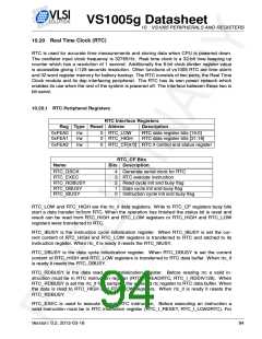
TIMER_CFG Bits
Bits Description
Name
TIMER_CFG_CLKDIV
7:0 Master clock divider
TIMER_CFG_CLKDIV is the master clock divider for all timer clocks. The generated internal
fm
clock frequency fi = c+1 , where fm is the master clock frequency and c is TIMER_CF_CLKDIV.
Example: With a 12 MHz master clock, TIMER_CF_DIV=3 divides the master clock by 4, and
12MHz
3+1
the output/sampling clock would thus be fi =
= 3MHz.
TIMER_ENA Bits
Bits Description
Name
TIMER_ENA_T2
TIMER_ENA_T1
TIMER_ENA_T0
2
1
0
Enable timer 2
Enable timer 1
Enable timer 0
Version: 0.2, 2012-03-16
92

 ETC [ ETC ]