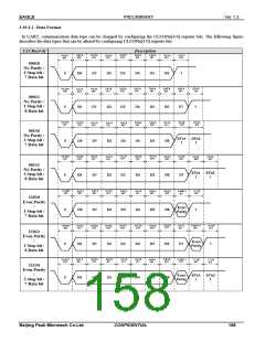
EAGLE
PRELIMINARY
Ver 1.3
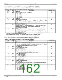
3.19.6 UART Channel 0~3 FIFO Control Register (UFCON0 ~ UFCON3)
Address : FFE0 8008h / FFE0 8028h / FFE0 8048h / FFE0 8068h
Bit
31 : 8
7 : 6
R/W
R
R/W
Description
Default Value
Reserved.
-
Receiver FIFO Trigger Level(RFTL)
00b
00 : 01 Byte
01 : 04 Byte
10 : 08 Byte
11 : 14 Byte
5 : 3
2
R
R/W
Reserved
XMIT FIFO Reset(XFR)
-
0b
When XFR is set to ‘1’, data in transmit FIFO is cleared but data in Shift
Register is not cleared and XFR is cleared automatically
1 : Resets transmit FIFO
1
0
R/W
R/W
RCVR FIFO Reset(RFR)
0b
0b
When XFR set to ‘1’, data in transmit FIFO is cleared but data in Shift
Register is not cleared and XFR is cleared automatically
1 : Resets Receiver FIFO
FIFO Enable
: when this Bit is set , transmit FIFO and receive FIFO is enabled
0 : 16450 UART Mode
1 : Enables FIFO
ULCON[7](Divisor Latch Access Bit) = DLAB
FIFO Control Register : (DLAB = 0) Register Write, (DLAB = 1) Register Read
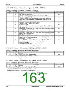
3.19.7 UART Channel 0~3 Line Control Register (ULCON0 ~ULCON3)
Address : FFE0 800Ch / FFE0 802Ch / FFE0 804Ch / FFE0 806Ch
Bit
31 : 8
7
R/W
R
R/W
Description
Default Value
Reserved.
-
0b
Divisor Latch Access Bit(DLAB)
: The read/write operation Divisor Latch Register and read FIFO Control
Register is allowed only when DLAB is set to on
Set Break(SB)
6
5
R/W
R/W
0b
0b
: Serial output value hold 1
Stick Parity(SP)
0 : Disables Stick Parity
1 : If PEN, EPS, SP are on, Parity Bit is ‘0’
If PEN, SP are on and EPS is zero , Parity Bit is ‘1’
Even Parity Select(EPS)
0 : Select Odd Parity
1 : Select Even Parity
Parity Enable(PEN)
0 : Disables Parity
1 : Enables Parity
Number of Stop Bits(STB)
0 : 1 Stop bit
4
3
2
R/W
R/W
R/W
0b
0b
0b
1 : 2 Stop bits (If you configure the WLS Bit 00b, then Number of Stop
bits is 1.5)
1 : 0
R/W
Word Length Select(WLS)
00 : 5 Bits/Character
00b
01 : 6 Bits/Character
10 : 7 Bits/Character
11 : 8 Bits/Character
Beijing Peak Microtech Co.Ltd.
CONFIDENTIAL
162

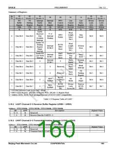
 ETC [ ETC ]