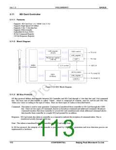
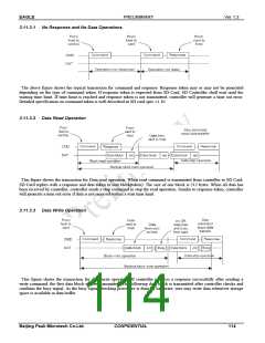
EAGLE
PRELIMINARY
Ver 1.3
3.10.8 USB PLL Control Register (UPLLCON)
Address : FFE0 2024h
Bit
31 : 9
8
R/W
R
R/W
Description
Default Value
Reserved
-
0b
Write Protect PLL Program Register (UPLLPMN)
0 : Write Disable.
1 : Write Enable.
7 : 5
4
R
R/W
Reserved.
Power Down Mode for UPLL
0 : UPLL Enable
-
1b
1 : UPLL Disable (Power Down)
Reserved.
3 : 0
R
-
3.10.9 USB PLL Program Register (UPLLPMN)
Address : FFE0 2028h
Bit
R/W
R
R/W
R/W
R/W
Description
Default Value
31 : 16
15 : 14
13 : 8
7 : 0
Reserved
-
Output frequency scaler value 2 bits (P)
Reference input frequency divider value 6 bits (M)
VCO frequency divider value 8 bits (N)
01b
02h
13h
Frequency equation : CLK_OUT = CLK_IN x (N+8) / ( (M+2) x 2^P )
Reference input frequency : Fin = 14.318MHz
Example : P = 01b, M = 000010b, N = 00110000 (100Mhz)
Refer Table 3-15
3.10.10 H264/MJPEG Clock Enable bit Register (HMCLKEN)
Address : FFE0 2030h
Bit
31 : 3
2
R/W
R
R/W
Description
Default Value
Reserved
MJPEG Clock Enable bit
0 : Disable
-
1b
1 : Enable
1
0
R/W
R/W
Scaler HCLK/SCK Clock Enable bit
0 : Disable
1 : Enable
H264 HCLK/SCK Clock Enable bit
0 : Disable
1b
1b
1 : Enable
Beijing Peak Microtech Co.Ltd.
CONFIDENTIAL
112

 ETC [ ETC ]