Ver 1.3
PRELIMINARY
EAGLE
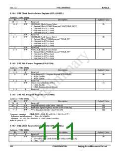
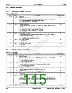
3.10.4 CRT Clock Source Select Register (CPLLCKSEL)
Address : FFE0 2010h
Bit
31 : 11
10 : 8
R/W
R
R/W
Description
Default Value
Reserved
CRTCLK2 Clock Source Select
-
0b
0 : External Clock VCLK2 from pad “CAPTURE_IN[3]”
1 : 2 divided by CPLL clock
2 : 4 divided by CPLL clock
4 : 8 divided by CPLL clock
Reserved
CRTCLK1 Clock Source Select
0 : External Clock VCLK from pad “VCLK_IN”
1 : 2 divided by CPLL clock
2 : 4 divided by CPLL clock
4 : 8 divided by CPLL clock
Reserved
H264_SCK Clock Source Select
0 : External Clock VCLK from pad “VCLK_IN”
1 : 2 divided by CPLL clock
2 : 4 divided by CPLL clock
4 : 8 divided by CPLL clock
7
6 : 4
R/W
R/W
-
0b
3
2 : 0
R/W
R/W
-
0b
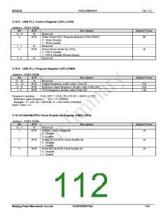
3.10.5 CRT PLL Control Register (CPLLCON)
Address : FFE0 2014h
Bit
31 : 9
8
R/W
R
R/W
Description
Default Value
Reserved
-
0b
Write Protect PLL Program Register (CPLLPMN)
0 : Write Disable.
1 : Write Enable.
7 : 5
4
R
R/W
Reserved.
Power Down Mode for CPLL
0 : CPLL Enable
-
1b
1 : CPLL Disable (Power Down)
3 : 0
R
Reserved.
-
3.10.6 CRT PLL Program Register (CPLLPMN)
Address : FFE0 2018h
Bit
R/W
R
R/W
R/W
R/W
Description
Default Value
31 : 16
15 : 14
13 : 8
7 : 0
Reserved
-
Output frequency scaler value 2 bits (P)
Reference input frequency divider value 6 bits (M)
VCO frequency divider value 8 bits (N)
01b
01h
0dh
Frequency equation : CLK_OUT = CLK_IN x (N+8) / ( (M+2) x 2^P )
Reference input frequency : Fin = 14.318MHz
Example : P = 01b, M = 000010b, N = 00110000 (100Mhz)
Refer to Table 3-15.
3.10.7 USB Clock Source Select Register (UPLLCKSEL)
Address : FFE0 2020h
Bit
31 : 1
0
R/W
R
R/W
Description
Default Value
Reserved
Clock Source Select
-
0b
0 : Slow clock (use clock divided by UPLLCON bit[2:0])
1 : UPLL clock
111
CONFIDENTIAL
Beijing Peak Microtech Co.Ltd.

 ETC [ ETC ]