EAGLE
PRELIMINARY
Ver 1.3
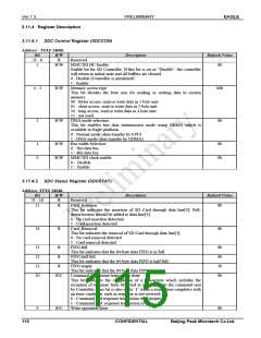
This bit indicates the completion of write operation. This bit is set to ‘1’
even when the write operation ends with a CRC error.
0 : Write operation is in progress or incomplete
1 : Write operation has completed
8
R/C
R/C
Read operation done
0b
This bit indicates the completion of read operation. This bit is set to ‘1’
even when the read operation ends with a CRC error.
0 : Read operation is in progress or incomplete
1 : Read operation has completed
7 : 6
Write CRC error code
00b
These bits represent the crc calculation result from SD Card for write
operation. SD Card checks the CRC for every block data received and
sends the result to controller.
00 : No transmission error
01 : Transmission error
10 : No CRC response ( Write data block is ignored in SD memory )
11 : Reserved
5
4
R/C
R/C
Response CRC error
This bit indicates a CRC error in response.
0 : No error
1 : Response CRC error occurred
Read data CRC error
0b
0b
This bit indicates a CRC error has occurred at the read data obtained from
SD Card.
0 : No error
1 : Read data CRC error occurred
3
2
1
0
R/C
R/C
R/C
R
Write data CRC error
This bit indicates a CRC error has occurred at the write data transmitted
to SD Card.
0 : No error
1 : Write data CRC error occurred
Response time out error
This bit indicates a time out error when response is not received within
the specified time limit.
0b
0b
0b
0b
0 : No error
1 : Command response was not received within specified time
Read data time out error
This bit indicates a time out error when read data is not received within
the specified time limit.
0 : No error
1 : The expected data from card was not received within specified time
Memory busy state
This bit represents the busy state of SD Card.
0 : Memory is ready
1 : Memory is busy
R/C represents Read and Clear . Writing ‘1’ to a Status register bit shall clear that bit to ‘0’.
Status[15:8] provides the interrupt source. Interrupt request shall be generated when one of these bits is set to ‘1’. The
interrupt request shall hold until the interrupt source is serviced.
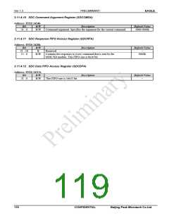
3.11.4.3 SDC Clock Divide Register (SDCCD)
Address : FFE0 2408h
Bit
31 : 10
9 : 0
R/W
R
R/W
Description
Default Value
Reserved.
-
MMC/SD clock Divide Register
200h
fAHB _ Clock
fSDCLK
=
2 + Divide [9: 0]
Beijing Peak Microtech Co.Ltd.
CONFIDENTIAL
116

 ETC [ ETC ]