AND8327/D
There are 2 loops we need to measure: one is a
combination of the fast and slow lanes observing the +12 V
output. The other one is the +5 V loop entering the TL431
via the slow lane.
We have mentioned before that measuring the loop at the
feedback input of the controller is not practical. As
demonstrated in Ref. [3], in order to correctly measure the
gain and phase of the feedback loop, the ac stimulus must be
injected between a low impedance node (on the power
supply output side) and a high impedance node (on the
control side). When the injection is done as described
previously, i.e. between the output of the power supply and
the feedback circuitry, the condition is optimal: the output
impedance of the observed point is low, and the input
impedance of the feedback path is high. But if we want to
open the loop between the optocoupler and the feedback pin
of the controller, the conditions are not favorable: the output
impedance of the optocoupler is high (this is the pull up
resistor in a common-emitter configuration), whereas the
input impedance of the FB pin can sometimes be affected by
internal dividers or pull-up resistors (it was 5 kW in our
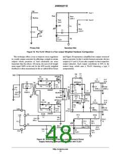
example). We can anyway find a way to perform this
measurement by inserting a buffer between the optocoupler
and the controller as Figure 21 illustrates. Using an NPN
transistor in a common-collector configuration, the output
impedance is made low compared to the input impedance of
the feedback pin.
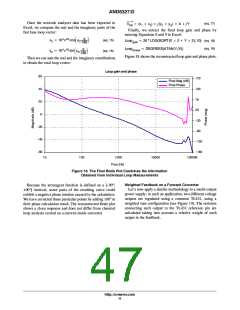
Figure 21. An NPN Buffer Allows Performing the
Loop Gain Measurement on the Primary Side
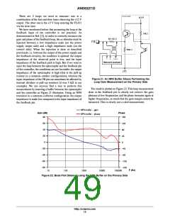
The result is plotted on Figure 22. This loop measurement
done at the feedback pin is clearly not correct: the gain
plateaus at low frequencies; and the phase increases again at
higher frequencies, so much that the gain margin cannot be
measured. This is clearly not a valid measurement.
NPN buffer - gain
NPN buffer - phase
Gain (dB)
Phase
80
180
135
90
60
40
20
45
0
0
-20
-40
-60
-80
-45
-90
-135
-180
F (Hz)
10
100
1000
10000
100000
Figure 22. Bode Plot Obtained using the NPN Buffer on the Primary Side
http://onsemi.com
13

 ETC [ ETC ]