AND8327/D
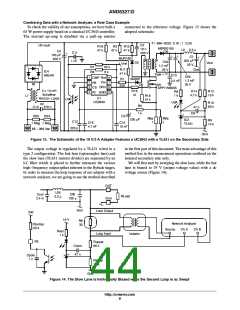
OUT
Gnd
Lfilt
2.2 m
Cfilt
100 m
RLoad
Loop Output
Network Analyzer
R6
33
Gnd
Ch B
Ch A
Source
Isolator
Loop Input
Vdd
DC Voltage
Rled
1 k
R7
20 k
~19 V
Rpullup
20 k
Rupper
66 k
FB
Czero
47 n
Cpole
1 n
Rlower
10 k
Gnd
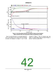
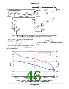
Figure 16. For the fast lane sweep, the slow lane is ac-decoupled from the converter output.
Care must be taken to avoid output runaway during this measurement!
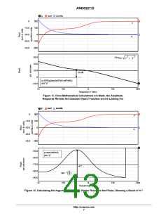
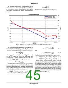
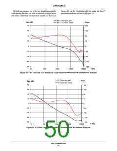
Figure 17 details the fast lane loop response. The power
stage pole f is around 20 Hz and corresponds to:
1
fpc
+
2pRpullupCpole
p
1
On Figure 13 schematic, C
resistor is R .
7
corresponds to C and the
11
pole
fp +
pRloadCout
R
pullup
After f , the power stage gain decreases with a -1 slope
p
until it reaches the 8 kHz pole formed by (R , C ) of
pullup pole
our type 2 compensator:
Fast lane loop response
180
144
108
72
100
80
fast lane - gain
fast lane - phase
60
40
36
20
0
0
-36
-72
-108
-144
-20
-40
-60
-80
-100
-180
1.00E+01
1.00E+02
1.00E+03
Freq (Hz)
1.00E+04
1.00E+05
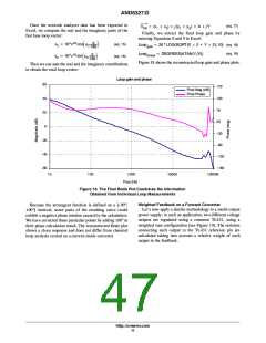
Figure 17. Fast Lane Loop Response Obtained with the Network Analyzer.
The Slow Lane is Externally Biased with a dc Power Supply
http://onsemi.com
10

 ETC [ ETC ]