AND8327/D
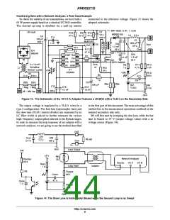
Combining Data with a Network Analyzer, a Real Case Example
To check the validity of our assumptions, we have built a
65ꢀW power supply based on a classical UC3843 controller.
The internal op-amp is disabled via a pull-up resistor
connected to the reference voltage. Figure 13 shows the
adopted schematic:
T1 86H-6232 0.18 : 1 : 0.25
C2
10 n
400 V
HV-bulk
R19
47 k
R3
47 k
R13
47 k
MBR20100
D5
L2 2.2 m
C4
100 mF
400 V
C11
+
+
+
C7
220 mF
25 V
+
MUR160
Vref
1 nF
C5a
1.2 mF
25 V
D2
Vout
+
-
R7
R6
20 k
6 k
R17
47 k
Gnd
IC4
KBU4K
Type = Y1
C13
2.2 nF
C5b
1.2 mF
25 V
1
2
3
4
8
7
6
5
Ref
CMP
1N4937
D8
R1
Vcc
DRV
GND
FB
CS
IN
M1
SPP11N60S5
R8
330
2 x 10 mH
Schaffner
RN122-1.5/02
R16
10
R14
4.7 k
R12
10 k
Rt
1 k
R18
47 k
L1
U1
UC3843
U3B
U3A
R10
56 k
X2
470 n
R5
1 k
C10
R23
47 n
C6
+
R24
C3
R6a
1
R6b
1
220 mF
IC2
TL431
R9
10 k
C12
220 p
C16
4.7 nF
C15
10 nF
1 Meg 1 Meg
85 - 260 Vac
Gnd
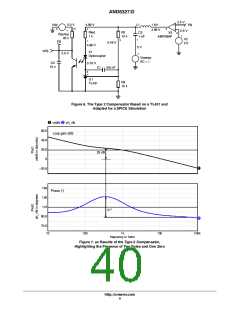
Figure 13. The Schematic of the 19 V/3 A Adapter Features a UC3843 with a TL431 on the Secondary Side
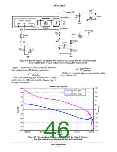
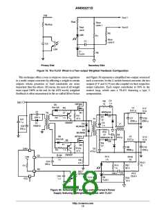
The output voltage is regulated by a TL431 wired in a
in the first part of this document. The main advantage of this
method lies in the measurement operations confined on the
isolated secondary side only.
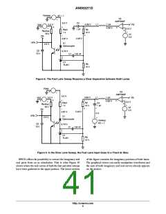
We will first start by sweeping the slow lane, while the fast
lane is biased to 19 V (output voltage value) with a dc
voltage source (Figure 14):
typeꢀ2 configuration. The fast lane (optocoupler lane) and
the slow lane (TL431 resistor divider) are separated by an
LC filter which is placed to further attenuate the various
high-frequency output spikes inherent to the flyback stages.
In order to measure the loop response of our adapter with a
network analyzer, we are going to use the method described
OUT
Lfilt
2.2 m
Cout
2.4 m
Cfilt
100 m
RLoad
Gnd
Gnd
Loop Output
Vdd
19 V
R6
33
Network Analyzer
Source Ch A Ch B
Rpullup
20 k
Rled
1 k
Loop Input
Isolator
FB
Rupper
66 k
Czero
47 n
Cpole
1 n
Rlower
10 k
Gnd
Figure 14. The Slow Lane is Individually Biased while the Second Loop is ac Swept
http://onsemi.com
8

 ETC [ ETC ]