AND8242/D
Over Power Compensation
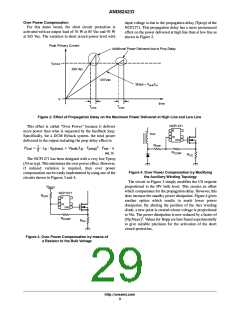
input voltage is due to the propagation delay (Tprop) of the
NCP1271. This propagation delay has a more pronounced
effect on the power delivered at high line than at low line as
shown in Figure 2.
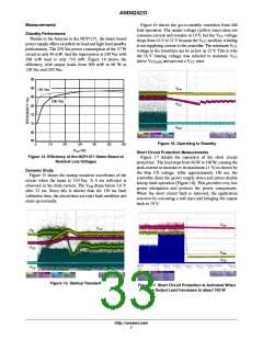
For this demo board, the short circuit protection is
activated with an output load of 76 W at 85 Vac and 93 W
at 265 Vac. The variation in short circuit power level with
Peak Primary Current
Additional Power Delivered due to Prop Delay
I
p(max)
230 Vac
120 Vac
Slope = V
/L
p
bulk
0
time
T
prop
T
prop
Figure 2. Effect of Propagation Delay on the Maximum Power Delivered at High Line and Low Line
NCP1271
This effect is called “Over Power” because it delivers
more power than what is requested by the feedback loop.
Specifically, for a DCM flyback system, the total power
delivered to the output including the prop delay effect is:
Aux
CS
DRV
R
OPP
1
2
P
+
@ L @ (I
p(max)
) V
ńL @ T
p
2 @ F @ h
(eq. 3)
out
p
bulk
prop)
sw
R
COMP
R
CS
The NCP1271 has been designed with a very low Tprop
(50 ns typ). This minimizes the over power effect. However,
if reduced variation is required, then over power
compensation can be easily implemented by using one of the
circuits shown in Figures 3 and 4.
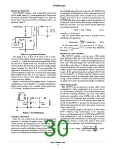
Figure 4. Over Power Compensation by Modifying
the Auxiliary Winding Topology
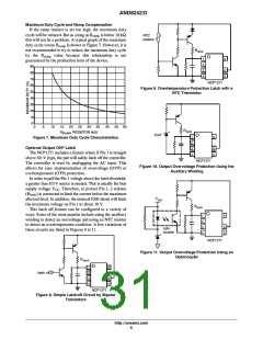
The circuit in Figure 3 simply modifies the CS setpoint
proportional to the HV bulk level. This creates an offset
which compensates for the propagation delay. However, this
does increase the standby power dissipation. Figure 4 gives
another option which results in much lower power
dissipation. By altering the position of the Aux winding
diode, a new point is created whose voltage is proportional
to Vin. The power dissipation is now reduced by a factor of
V
BULK
NCP1271
R
OPP
CS
DRV
2
R
COMP
(Np:Naux) . Values for Ropp are best found experimentally
to give suitable precision for the activation of the short
circuit protection.
R
CS
Figure 3. Over Power Compensation by means of
a Resistor to the Bulk Voltage
http://onsemi.com
3

 ETC [ ETC ]