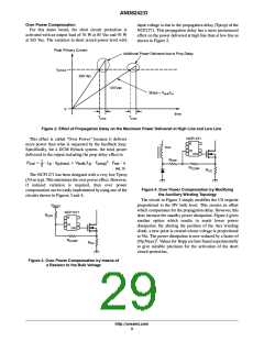
AND8242/D
Layout Consideration
It is important to note that when Pin 1 is open it sets the
default skip level to 1.2 V. However, in this mode, pin 1 is
internally pulled high to the Vskip-reset level (6.5 V typ).
This only leaves about 1.5 V of noise margin before the part
latches off. Therefore, if a skip level of 1.2 V is desired, then
instead of leaving pin 1 open, it is always recommended to
place a 28 kW resistor from pin 1 to GND. Then the skip level
becomes 1.2 V (28 kW x 43 mA = 1.2 V), and the pin 1
voltage is also 1.2 V. This gives much better noise immunity
and reduces the chance of falsely triggering the latch due to
noise or leakage current from the external latch circuitry.
Additionally, a small capacitor should be added to pin 1 to
further increase the noise immunity.
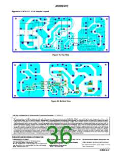
Figures 9-10 show the layout of the design. It is a
single-layer PCB. As with any power converter, some care
must be exercised with the design and layout. The following
are some important guidelines.
1. Minimize the high-current loop and locate the IC
controller outside the high-current loop to prevent
malfunctioning of the IC internal logic due to
strong magnetic fields from the high current.
2. Locate the decoupling capacitors close to the
device to improve noise immunity.
3. Locate the V capacitor very close to the device
CC
to prevent the circuit from entering a UVLO fault
condition because of noise.
HV Pin Protection Circuit
4. Locate the output voltage sense resistor close to
the output load points.
5. Minimize the current sense trace. It can become
easily polluted with noise.
6. Minimize the distance between the feedback
opto-coupler and controller because this trace is
also easily polluted.
7. Minimize the distance between the MOSFET and
controller because the PCB trace is high frequency
and high current so it can easily pollute other parts
of the circuit.
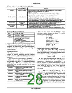
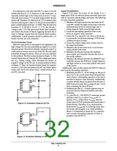
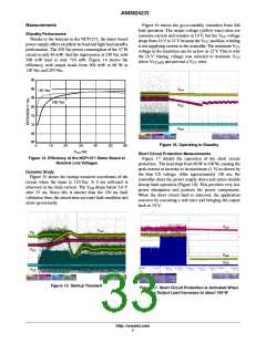
When the main power is interrupted in the application, the
high voltage DC bus may potentially go negative in a short
transient period. Since this is directly connected to pin 8, it
could create a reverse current out of the HV Pin and could
potentially damage the device. There are two easy solutions
to this problem. The first is demonstrated in Figure 12. The
inserted diode turns on when the HV Pin voltage goes below
the V
biasing voltage. This eliminates the chance of
CC
negative voltage on the HV pin. A second method is shown
in Figure 13. Here, the inserted resistor limits the negative
current to a low level and protects the HV pin. Either option
works well, but for this demo board, a diode between V
and HV was used.
Additionally, there are three pins in the NCP1271 that may
need external decoupling capacitors.
CC
1. Skip/latch pin (Pin 1) – If the voltage on this pin is
above 8.0 V, the circuit enters latch-off protection
mode. Hence, a decoupling capacitor on this pin is
essential to improve noise immunity. Additionally,
a resistor should always be placed from this pin to
GND to prevent noise from causing the pin 1 level
from exceeding the latch-off level.
2. Feedback pin (Pin 2) – A small capacitor may be
necessary here for improved stability and noise
immunity.
HV
1N4005
1
2
3
4
8
Vcc
6
5
NCP1271
3. V pin (Pin 6) – The NCP1271 maintains normal
CC
operation when V is above V
(9.1 V
, then the
CC
typical). If V drops below V
CC(off)
CC
CC(off)
circuit enters UVLO protection and restarts after a
double hiccup. Therefore, if VCC inadvertently
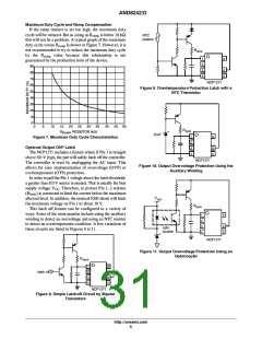
Figure 12. Protection Diode for HV Pin
drops below V
due to switching noise, then
the circuit will recognize it as a fault condition.
CC(off)
Hence, it is important to locate the V capacitor
CC
>4.7 kW
and a ceramic decoupling capacitor as close as
possible to the NCP1271.
HV
1
2
3
4
8
Vcc
6
5
NCP1271
Figure 13. Protection Resistor on HV Pin
http://onsemi.com
6

 ETC [ ETC ]