AND8318/D
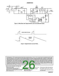
Another consequence of the tapped inductor is an
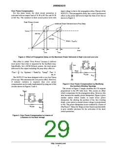
half that of the peak−to−peak current step. This is
significantly greater than the rather “benign” triangle
current waveform that the conventional buck output
capacitor typically experiences. Depending on the capacitor
ESR, it may be necessary to use multiple output capacitors
in parallel not only to handle the increased ripple current but
to also keep the peak−to−peak voltage ripple component
appearing across the capacitor’s ESR under control. For
applications requiring very low output ripple, it may be
necessary to use a two−stage ”pi” network output filter with
the addition of a small 4.7 mH slug inductor and another
output capacitor following it.
additional negative voltage excursion on the source terminal
of the switching MOSFET in U1 because the freewheel
diode is now unable to directly clamp this voltage to a diode
drop below the output common rail. The additional negative
voltage seen by the MOSFET will be the buck output voltage
plus diode drop times the turns ratio of the full inductor
winding with respect to the freewheel winding, or (12 + 0.8)
x 4 = 52 volts approximately. The leakage inductance
between the windings will also contribute a narrow spike
which could have a similar amplitude or higher. With the
multifilar coil winding techniques described above this
spike should be minimal; however, depending on the
MOSFET’s voltage rating, an optional small R/C snubber
(R4 & C8) from the switching node to the output common
should all but eliminate the spike. Assuming a universal
mains input at high line (270 Vac), the peak voltage seen by
the MOSFET will be in the order of 500 volts or less which
is well below the 700 volt rating of the NCP1014.
References
NCP1014 Data Sheet; ON Semiconductor Website
(www.onsemi.com)
ON Semiconductor Design Notes DN06002, DN06011;
ON Semiconductor Website
“Modern DC−to−DC Switchmode Power Converter
Circuits”, Chapter 8; By Rudolf Severns and Gordon
Bloom; Van Nostrand Reinhold
ON Semiconductor Application Notes AND8190,
AND8226; ON Semiconductor Website
One other issue that should be mentioned which is
affected by the tapped inductor is the ripple current rating of
output capacitor C4. The abrupt current step in the inductor
current at the moment of MOSFET turnoff will be seen by
the capacitor and the rms value will be approximately one
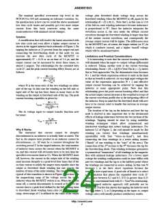
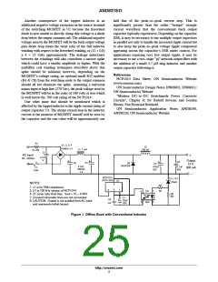
R1
D1, 2, 3, 4
L2
750 uH
1N4007 x 4
L1, 1 mH
15, 2W
C1
AC input
+
4.7nF
”x”
85 − 265Vac
Output
12 V,
300 mA
C5
C3
C2
D5
MUR160
C4
470uF
25V
4.7uF,
400Vdc
x 2
0.1uF
50V
F1
0.5A
_
NCP1014
(SOT−223)
Z1 = 11V
(Vset)
U1
NOTES:
4
2
R2
39
1. L1 is for EMI compliance.
3. U1 is 100 kHz version of NCP1014.
4. Z1 zener sets Vout max: Vout = Vz + 0.85V.
7. Crossed schematic lines are not connected.
8. CAUTION: Output is not isolated from AC input
and represents lethal hazard.
1
3
U2
1
2
4
R3
390
C7
33uF
25V
C6
+
3
opto
1nF
Figure 1. Offline Buck with Conventional Inductor
http://onsemi.com
3

 ETC [ ETC ]