AND8242/D
Biasing the Controller
bunch of skip pulses. To address this need, the NCP1271 has
a proprietary Soft-Skip feature which ramps each bunch of
pulses. This dramatically lowers acoustic noise and allows
a higher skip level to be set for greater power savings. The
NCP1271 also allows the designer to select the optimal level
of the peak current during skip through a simple resistor
from pin 1 to GND. This skip resistor sets the skip level
according to equation 4:
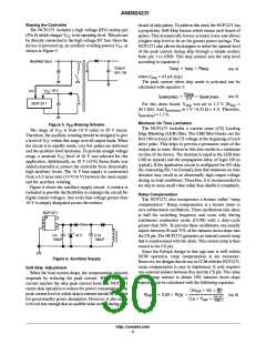
The NCP1271 includes a high voltage (HV) startup pin
(Pin 8) which charges V to its operating level. This pin can
CC
be directly connected to the high voltage DC bus. Once the
device is powered up, an auxiliary winding powers V as
CC
shown in Figure 5.
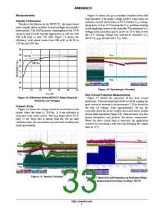
Rectified Input
Output
V
+ I R
skip skip
(eq. 4)
skip
19V / 3A
where I
= 43 mA (typ)
skip
The peak current when skip mode is activated can be
calculated with equation 5:
V
CC
16 V
HV
V
skip
3ꢀV
I
+
I
peak(max)
(eq. 5)
peak(skip)
NCP1271
For this demo board, V
30.1 kW). And I
was set to 1.3 V (R
=
is 1 V / 0.25 W = 4 A. Therefore,
skip
skip
peak(max)
I
) = 1.7 A.
peak(skip
Minimum On Time Limitation
Figure 5. VCC Biasing Scheme
The NCP1271 includes a current sense (CS) Leading
Edge Blanking (LEB) filter. The LEB filter blanks out the
first 180 ns (typ) of the CS voltage at the beginning of each
drive pulse. This helps to prevent a premature reset of the
output due to noise. However, this also results in a minimum
on time of the device. The duration is equal to the LEB time
(180 ns typical) and the propagation delay of logic (50 ns
typical). If the application circuit is configured for 0% skip
(by connecting Pin 1 to Ground), then that minimum on time
duration may result in an abnormally high output voltage
during no load conditions. Therefore, it is recommended to
set skip to some small value rather than disable it completely.
The range of V is from 10 V (min) to 20 V (max).
CC
Therefore, the auxiliary winding should be designed to give
a level of V within this range over all output loads. When
CC
the circuit is in standby mode, very few pulses are delivered
and the auxiliary level decreases. To provide enough voltage
range, a nominal V level of 16 V was selected for this
CC
application. Additionally, an 18 V ( 5%) Zener diode was
added externally to protect the controller from abnormally
high auxiliary levels. The 16 V bias supply is constructed
from a 6:5 turns ratio (19 V:16 V) between the main output
and the auxiliary winding.
Figure 6 shows the auxiliary supply circuit. A resistor is
included to provide the flexibility to redesign the circuit for
higher output voltages. Any extra bias voltage greater than
18 V is simply dissipated across the resistor.
Ramp Compensation
The NCP1271 also incorporates a feature called “ramp
compensation.” Ramp compensation is a known mean to
cure subharmonic oscillations. These oscillations take place
at half the switching frequency and occur only during
continuous conduction mode (CCM) with a duty-cycle
greater than 50%. To prevent these oscillations, one usually
injects between 50 and 75% of the inductor down slope into
the CS pin. The NCP1271 generates an internal current ramp
that is synchronized with the clock. This current ramp is then
routed to the CS pin.
NCP1271
C4
100uF
18 V
C13
100uF
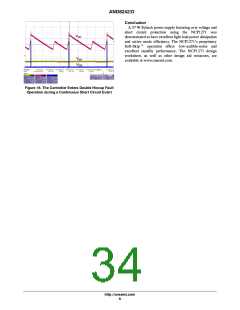
Since the flyback design in this app note is well within
DCM operation, ramp compensation is not necessary.
However, for designs that do run in CCM with the NCP1271,
ramp compensation is easy to implement. It only requires
one external resistor between Rcs and the CS pin. The value
of the ramp resistor to obtain 50% inductor down slope
injection can be calculated with the following equation:
Figure 6. Auxiliary Supply
Soft-Skip Adjustment
When the load current drops, the compensation network
responds by reducing the peak current. When the peak
current reaches the skip peak current level, the NCP1271
enters skip operation to reduce the power consumption. The
peak current level at which skip is entered should be set high
for good standby power dissipation. However, it also needs
to be set low enough that no audible noise occurs during each
N
P
ǒ(V
Ǔ
) V )
out
f
N
S
R
+ 0.50 R
CS
(eq. 6)
ramp
100ꢀmA
ǒLp F
Ǔ
sw
0.80
http://onsemi.com
4

 ETC [ ETC ]